Logic device and method supporting scan test

a logic device and scan technology, applied in the field of scan testing systems and methods, can solve the problems of reducing the performance of the logic circuit, consuming more power during normal non-test operation, and consuming less power during pulsed latches, so as to reduce the delay in the data path, reduce the delay, and consume less power.

Active Publication Date: 2007-12-27
QUALCOMM INC
View PDF9 Cites 40 Cited by
  • Summary
  • Abstract
  • Description
  • Claims
  • Application Information

AI Technical Summary

Benefits of technology

[0013]One particular advantage provided by embodiments of the particular logic device is that the test logic is removed from the data path of the logic device, reducing delays in the data path. In one particular embodiment, the delays may be reduced by up to 25 percent.
[0014]Another advantage is provided in that the logic device may consume less power than a conventional logic device with design for testability (DFT) features in the critical data path. Since the test ...

Problems solved by technology

Unfortunately, to provide the data to the input, the test logic, such as a multiplexer, is typically placed within the data path of the logic circuit and may unnecessarily consume power during normal non-test operation.
Moreover, such test logic may introduce delays i...

Method used


Image

  • Logic device and method supporting scan test
  • Logic device and method supporting scan test
  • Logic device and method supporting scan test

Examples


Embodiment Construction

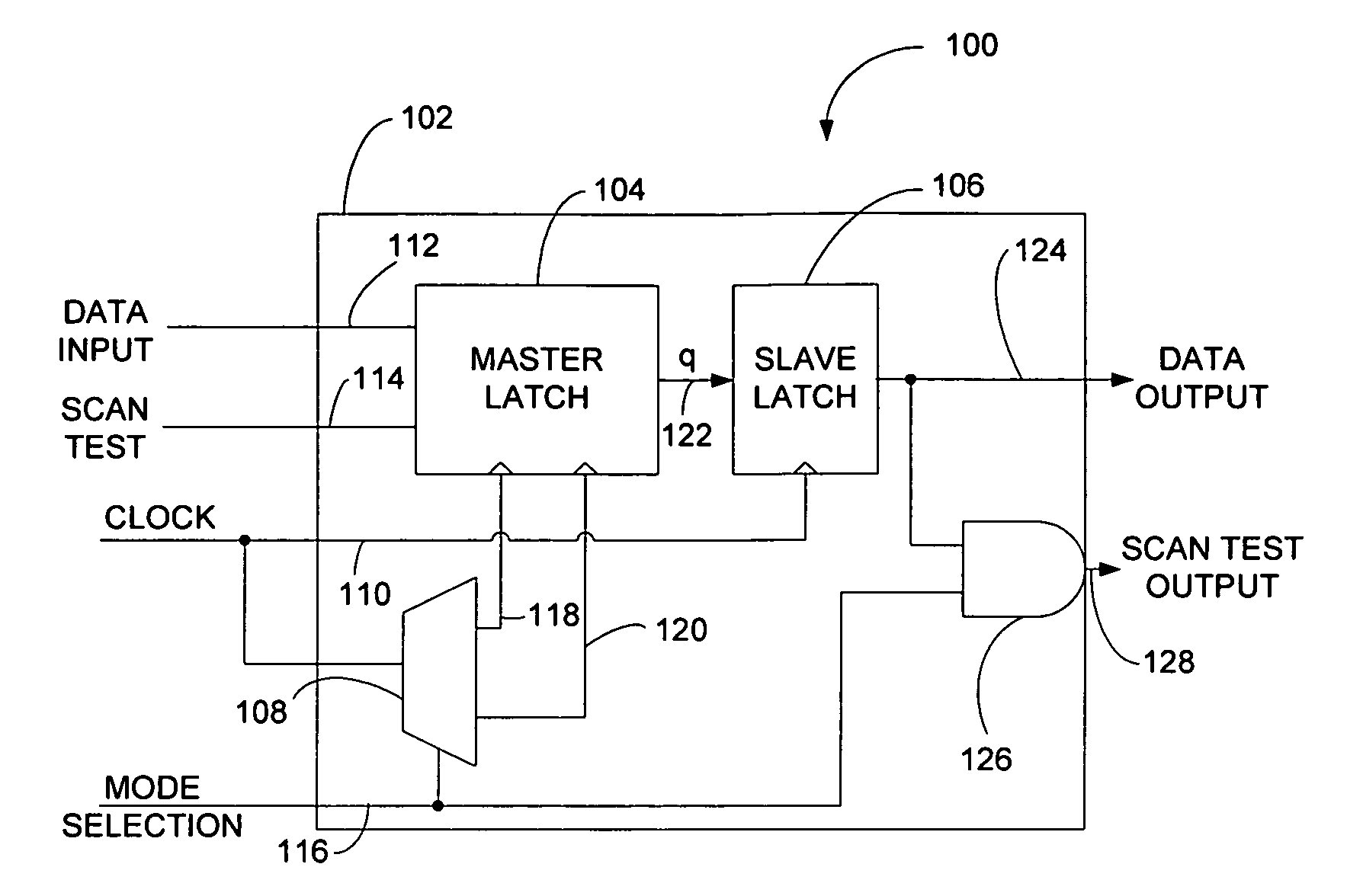
[0023]FIG. 1 is a block diagram of a logic device 100 with design for testability (DFT) compatible test logic. The logic device 100 includes an integrated circuit 102 that includes a master latch 104, a slave latch 106, and a clock demultiplexer 108. The integrated circuit 102 includes a clock input 110, a data input 112, a scan test input 114, and a mode selection input 116. The clock demultiplexer 108 receives the clock input 110 and a mode selection input 116. The clock demultiplexer 108 is responsive to the clock input 108 to selectively provide a first clock output 118 and a second clock output 120. The master latch 104 is coupled to the data input 112 and to the scan test input 114. The master latch 104 also includes an output 122. The master latch 104 is responsive to the first clock output 118 of the clock demultiplexer 108 and the second clock output 120 of the clock demultiplexer 108 to selectively couple the data input 112 or the scan test input 114 to the output 122. In ...


PUM


Abstract

A logic device includes a data input, a scan test input, a clock demultiplexer, and a master latch. The clock demultiplexer is responsive to a clock input to selectively provide a first clock output and a second clock output. The master latch is coupled to the data input and to the scan test input and includes an output. The master latch is responsive to the first clock output of the clock demultiplexer and the second clock output of the clock demultiplexer to selectively couple the data input or the scan test input to the output.

Description

BACKGROUND[0001]I. Field[0002]The present disclosure generally relates to systems and methods of scan testing.[0003]II. Description of Related Art[0004]Generally, an integrated circuit may include multiple digital logic circuits. One type of digital logic circuit is a flip-flop, which is a circuit that can be switched between two states. Flip-flop circuits are a common type of sequential circuit element used to build digital systems. Accordingly, flip-flop circuits may have an impact on both power and performance for such systems.[0005]Modern integrated circuits usually incorporate a variety of design-for-test (DFT) structures to enhance their inherent testability. Typically, the DFT structures are based on a scan design, where scan test data is provided to a test pin or where a plurality of externally accessible scan chains are embedded into the integrated circuit. When the scan chain is embedded, the scan chain may include one or more scan cells coupled in series, with each scan c...

Claims


Application Information

Patent Timeline
IPC IPC(8): G01R31/28
CPCG01R31/3025G01R31/318575G01R31/318552G01R31/3177G01R31/3185
Inventor SAINT-LAURENT, MARTINBASSETT, PAULPATEL, PRAYAG
Owner QUALCOMM INC
Why Eureka
Try Eureka