
Operation method of flash memory device capable of down-shifting a threshold voltage distribution of memory cells in a post-program verify operation

a technology of flash memory and threshold voltage distribution, which is applied in the direction of digital storage, static storage, instruments, etc., can solve the problem of difficulty in down-shifting the threshold voltage distribution

Active Publication Date: 2010-08-24
SK HYNIX INC
View PDF9 Cites 29 Cited by
  • Summary
  • Abstract
  • Description
  • Claims
  • Application Information

AI Technical Summary

Benefits of technology

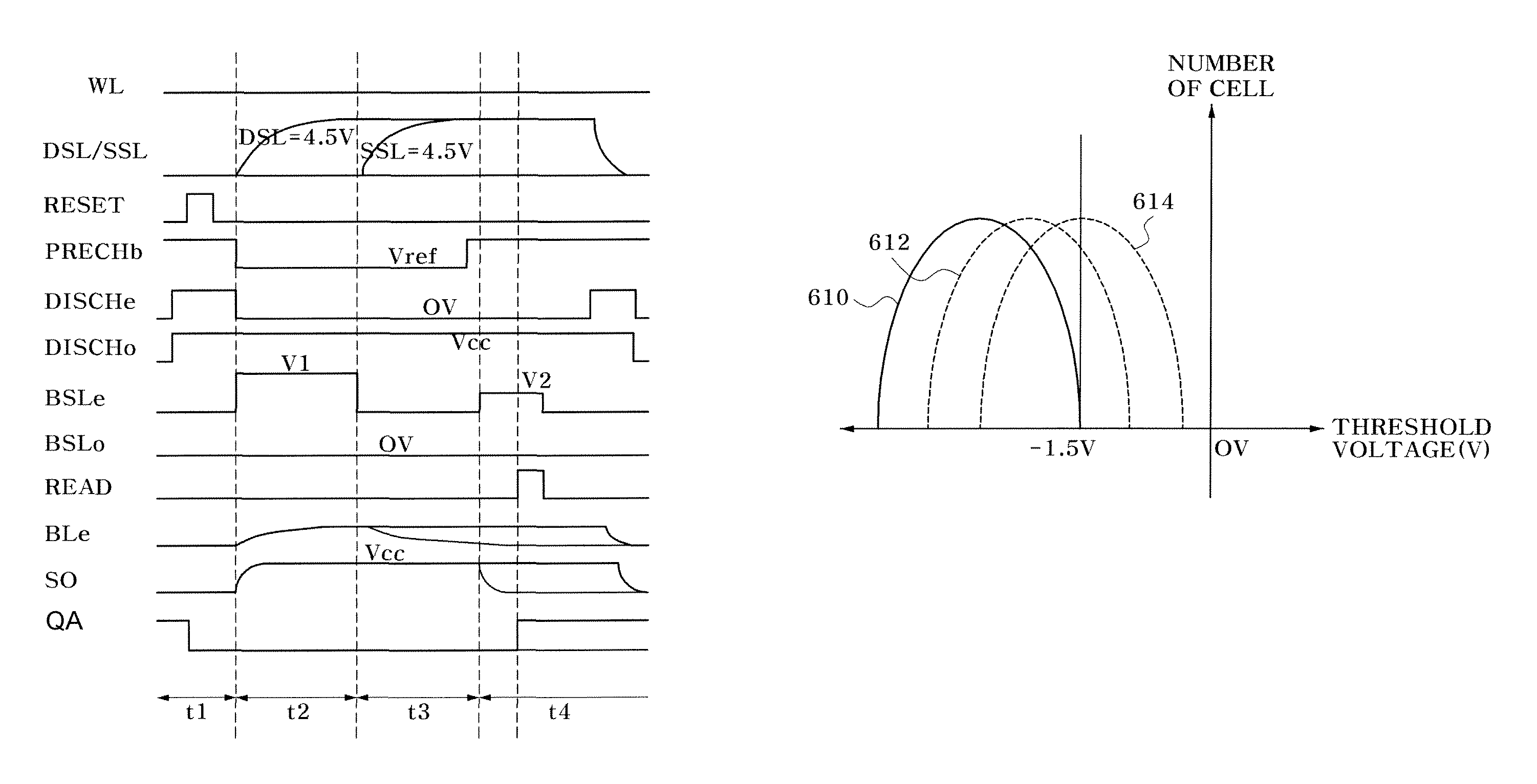
[0011]Embodiments of the invention are directed to a driving method of a flash memory device, which is capable of preventing program failure such as those caused by a shift of a threshold voltage distribution due to a program disturb or a program stress after an erase operation by achieving the effect that a verify level is down-shifted through an increase in a sensing current during a post-program verify operation.

Problems solved by technology

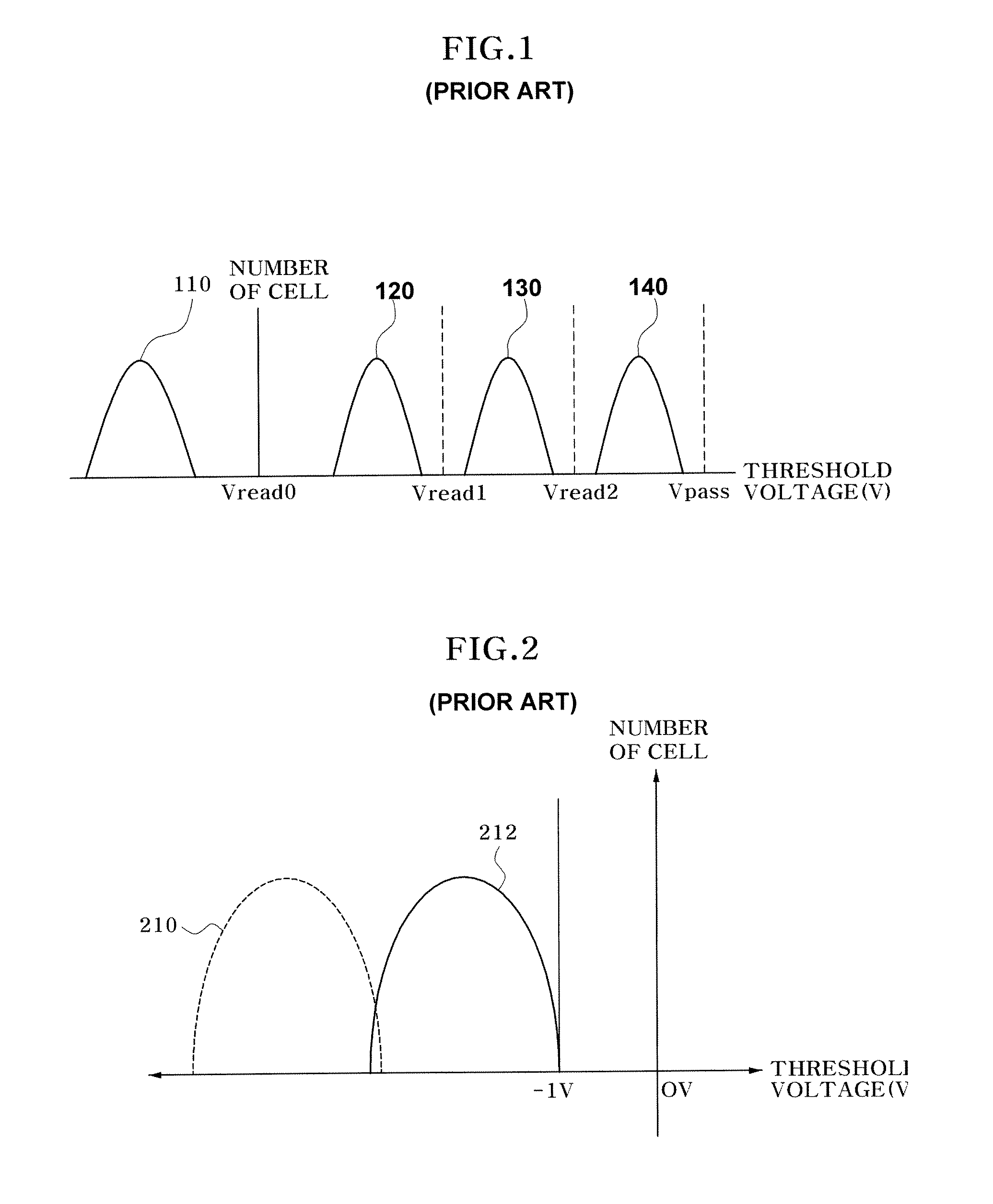
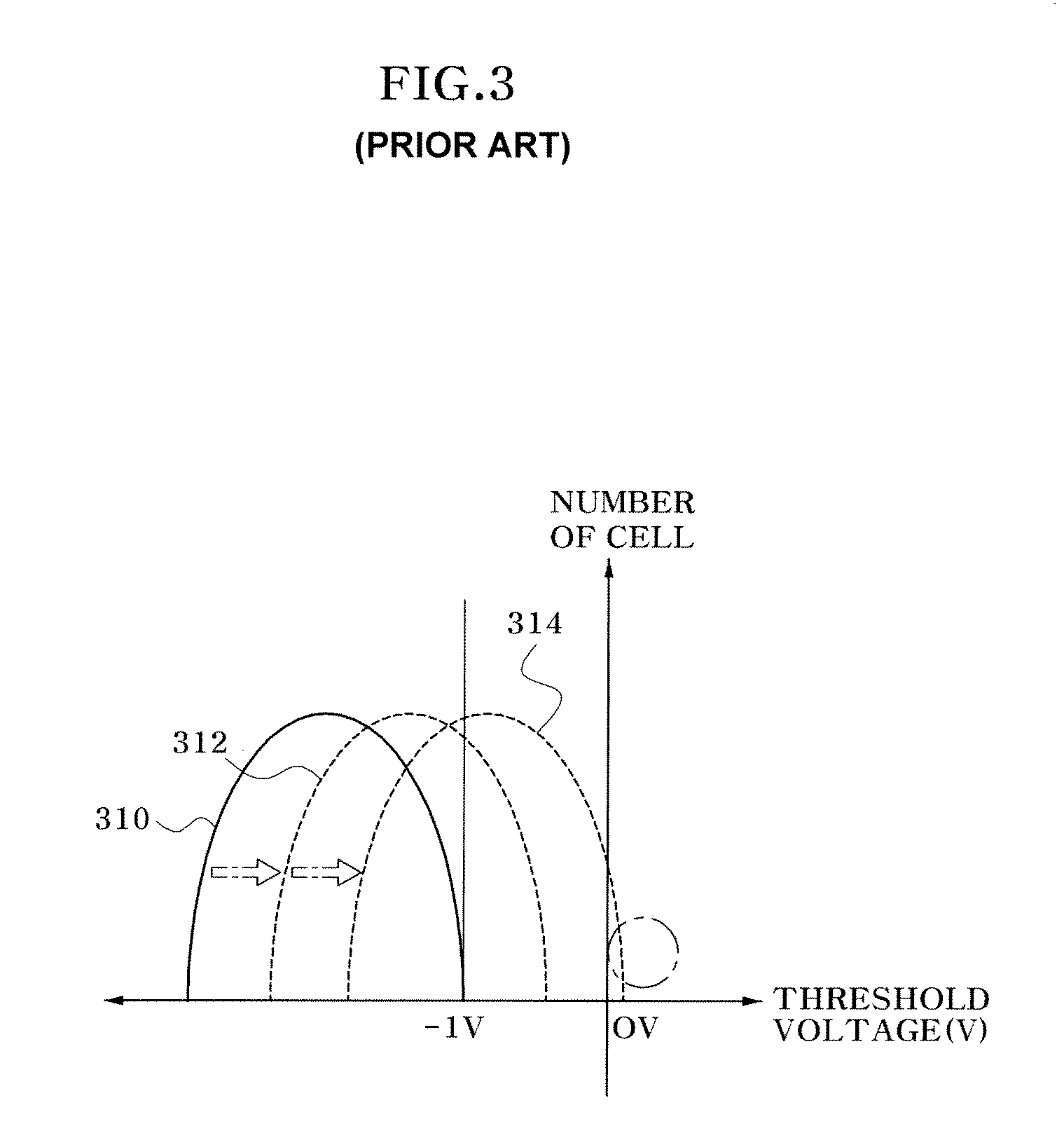
The threshold voltage distribution of the memory cell may be shifted, thereby cause failure due to a program disturb or a program stress.
Accordingly, it is difficult to down-shift the threshold voltage distribution obtainable by a typical post-program operation to a level less than about −1 V.

Method used


Image

  • Operation method of flash memory device capable of down-shifting a threshold voltage distribution of memory cells in a post-program verify operation
  • Operation method of flash memory device capable of down-shifting a threshold voltage distribution of memory cells in a post-program verify operation
  • Operation method of flash memory device capable of down-shifting a threshold voltage distribution of memory cells in a post-program verify operation

Examples


Embodiment Construction

[0023]In an embodiment of the invention, during a post-program operation for reducing a threshold voltage of an erased cell, a threshold voltage of a memory cell is higher than its actual value if a sensing current Itrip increases in a program verify operation. This enables a verify level to be relatively lowered, which provides the effect that the threshold voltage distribution of the memory cell is down-shifted after the post-program is completed.

[0024]The magnitude of the sensing current Itrip flowing from a NAND string 411 of a cell array 410 (as shown in FIG. 4) to a sensing node SO of a page buffer 420 through a bit line 412 may be calculated from Eq. 1 below.

Itrip=(CBL×(V1−V2)) / tEVAL  (Eq. 1)

[0025]where Itrip is the sensing current, CBL is a bit line capacitance, V1 and V2 are voltages applied to bit line select or unselect signals BSLe and BSLo (as shown in FIG. 4), and tEVAL is an evaluation time. As shown in Eq. 1, the sensing current Itrip may be increased if V1 increases...


PUM


Abstract

In a driving method of a flash memory device including a selected first bit line and an unselected second bit line, a program voltage of a pulse is applied to word lines of all memory cells in a block passing an erase verify operation. After the first and second bit lines are precharged to a predetermined level, a ground voltage is applied to the word lines of all the memory cells in the block. The memory cells are evaluated for a predetermined time shorter than an evaluation time of a read operation. Whether or not a memory cell passing a verify operation exists among the memory cells is sensed. Resultantly, when the memory cell passing the verify operation exists, the memory cells in the block are programmed to a desired level using a predetermined program voltage and a step voltage.

Description

CROSS-REFERENCE TO RELATED APPLICATIONS[0001]This patent claims priority to Korean application number 10-2007-0065838, filed on Jun. 29, 2007, the disclosure of which is incorporated by reference in its entirety.TECHNICAL FIELD[0002]This patent relates to flash memory devices, and more particularly, to a driving method of a flash memory device, which is capable of preventing program failure by down-shifting a threshold voltage distribution of a memory cell in a post-program verify operation.BACKGROUND OF THE INVENTION[0003]Among various types of flash memory device, NAND-type flash memory devices are increasingly used as a high-capacity data storage media. To meet the demand for the high-capacity memory devices with high-integration, a multi-level cell (MLC) structure for the flash memory devices has recently been proposed, which is capable for increasing the data storage capacity in a smaller chip size. Generally, a single level cell (SLC) includes two states, i.e., a programmed st...

Claims


Application Information

Patent Timeline
Patent Type & Authority Patents(United States)
IPC IPC(8): G11C11/34G11C16/04
CPCG11C16/0483G11C16/3454G11C16/34G11C16/30G11C16/12
Inventor KIM, JUN INLEE, JU YEAB
Owner SK HYNIX INC
Learn More