Simultaneous irradiation of a substrate by multiple radiation sources

a radiation source and simultaneous irradiation technology, applied in the direction of polycrystalline material growth, crystal growth process, gel state, etc., can solve the problems of insufficient insufficient heating of wafer regions, and inability to achieve thermal equilibrium over length scales, so as to improve the spatial uniformity of thermal annealing of silicon wafers

Inactive Publication Date: 2010-09-07
GLOBALFOUNDRIES INC
View PDF23 Cites 5 Cited by
  • Summary
  • Abstract
  • Description
  • Claims
  • Application Information

AI Technical Summary

Benefits of technology

[0022]The present invention advantageously improves the spatial uniformity of thermal annealing of silicon wafers.

Problems solved by technology

When electromagnetic radiation is incident on these stacks, constructive and destructive interference occur due to reflections at each interface in the path of the incident radiation.
Thus the wafer regions are not heated uniformly in these circumstances.
State-of-the-art thermal processing employs electromagnetic radiation on time scales below 0.1 s and as a result thermal equilibrium is not achieved over length scales that are smaller than a typical Very Large-Scale Integration (VLSI) die size.

Method used


Image

  • Simultaneous irradiation of a substrate by multiple radiation sources
  • Simultaneous irradiation of a substrate by multiple radiation sources
  • Simultaneous irradiation of a substrate by multiple radiation sources

Examples


Embodiment Construction

1. Introduction

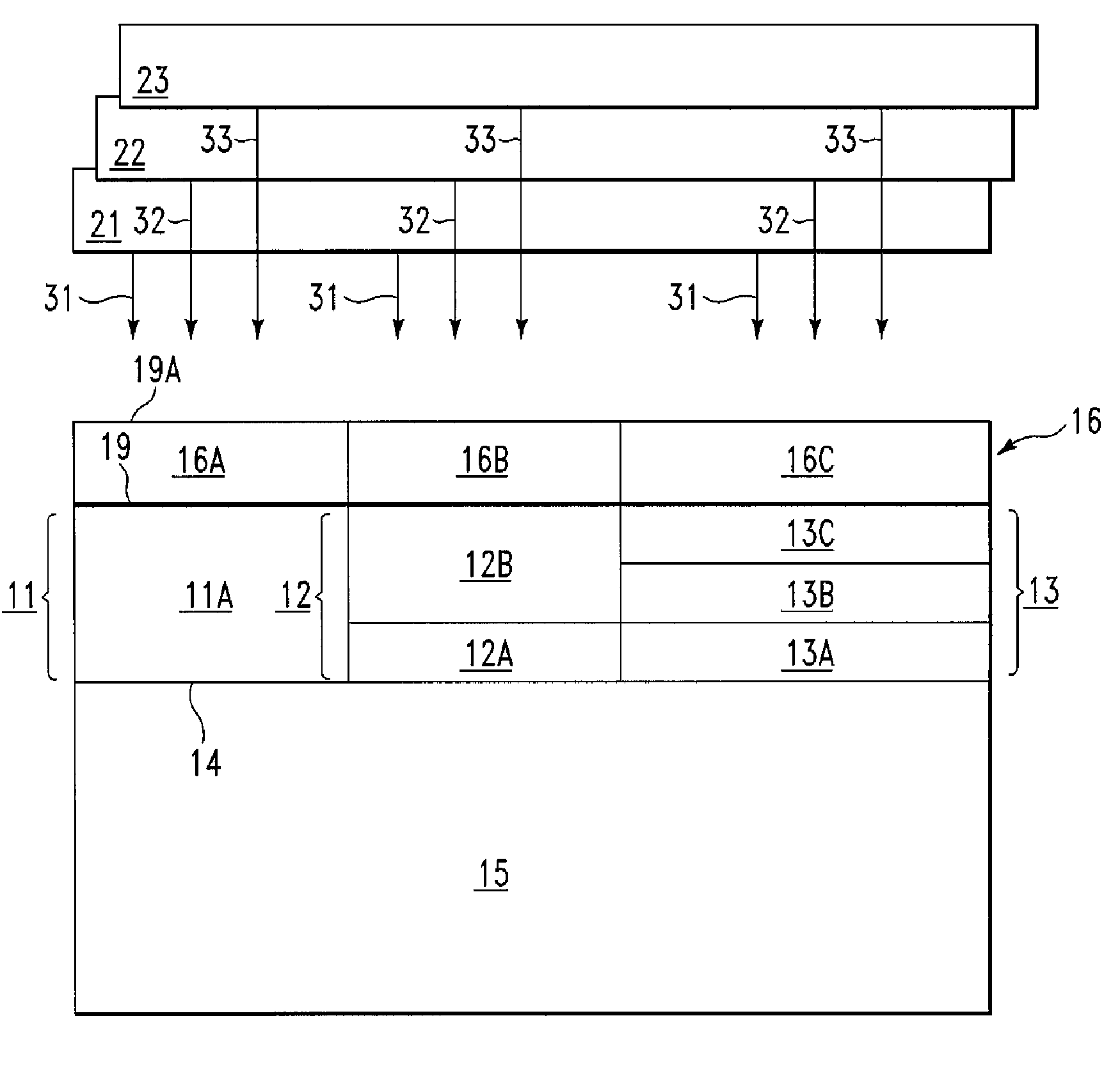
[0034]FIG. 1 depicts a front cross-sectional view of a substrate 10 with radiation sources 21, 22, and 23 adapted to irradiate the substrate 10 with electromagnetic radiation 31, 32, and 33, respectively, in accordance with embodiments of the present invention. The radiation 31, 32, and 33 is incident on the top surface 19 of the substrate 10. The substrate 10 comprises a base layer 15 and layered stacks 11, 12, and 13 on and in direct mechanical contact with the base layer 15. The base layer 15 may comprise comprises a dielectric material, a semiconductor material, a metal, an alloy, etc. For example, the base layer 15 may be a semiconductor layer (e.g., a semiconductor wafer) comprising a semiconductor material (e.g., single crystal silicon, polysilicon, germanium, etc.—doped or undoped). The substrate 10 may terminate with the base layer 15. Alternatively the base layer 15 may be disposed between the stacks 11-13 and one or more additional layers of the substrate.

[...


PUM

PropertyMeasurementUnit
power distributionaaaaaaaaaa
wavelengthaaaaaaaaaa
incident energy fluxaaaaaaaaaa

Abstract

A method for configuring J electromagnetic radiation sources (J≧2) to simultaneously irradiate a substrate. Each source has a different function of wavelength and angular distribution of emitted radiation. The substrate includes a base layer and I stacks (I≧2) thereon. Pj denotes a same source-specific normally incident energy flux on each stack from source j. For simultaneous exposure of the I stacks to radiation from the J sources, Pj is computed such that an error E being a function of |W1−S1|, |W2−S2, . . . , |WI−SI| is about minimized with respect to Pj=1, . . . , J). Wi and Si respectively denote an actual and target energy flux transmitted into the substrate via stack i (i=1, . . . , I). The stacks are exposed to the radiation from the sources characterized by the computed Pj (j=1, . . . , J).

Description

RELATED APPLICATION[0001]This application is related to U.S. patent application Ser. No. 11 / 427,419 entitled “SERIAL ILLUMINATION OF A SUBSTRATE BY MULTIPLE RADIATION SOURCES”, filed on Jun. 29, 2006, and hereby incorporated by reference.FIELD OF THE INVENTION[0002]The present invention relates generally to irradiation of a substrate and more particularly to simultaneous irradiation of a substrate by multiple radiation sources.BACKGROUND OF THE INVENTION[0003]Rapid thermal anneal (RTA) is used in semiconductor device fabrication to heat a wafer to alter the wafer's properties, such as to activate dopants, repair damage from ion implantation, transport dopants in or out of the wafer or to other locations within the wafer, etc.[0004]Rapid thermal anneal of a silicon wafer is often effected through direct exposure of the wafer to electromagnetic radiation. Annealing is usually performed after patterning of multiple stacks of dielectric layers on the silicon wafer. When electromagnetic ...

Claims


Application Information

Patent Timeline
Patent Type & Authority Patents(United States)
IPC IPC(8): H01L21/00C30B25/00
CPCH01L21/268Y10T117/1004
Inventor ANDERSON, BRENT ALANNOWAK, EDWARD JOSEPH
Owner GLOBALFOUNDRIES INC
Why Eureka
Try Eureka