Accommodating device for accommodation and mounting of a wafer

A technology for accommodating devices and wafers, used in the manufacture of electrical components, circuits, semiconductor/solid-state devices, etc., and can solve problems such as affecting process quality and hindering photoresist removal.

Inactive Publication Date: 2015-06-17
イーヴィーグループインコーポレイテッド
View PDF5 Cites 2 Cited by
  • Summary
  • Abstract
  • Description
  • Claims
  • Application Information

AI Technical Summary

Problems solved by technology

This in turn can impede photoresist removal or otherwise affect process quality during the finishing process

Method used


Image

  • Accommodating device for accommodation and mounting of a wafer
  • Accommodating device for accommodation and mounting of a wafer
  • Accommodating device for accommodation and mounting of a wafer

Examples


Embodiment Construction

[0035] The same elements or elements fulfilling the same function are marked by the same reference numerals in the figures.

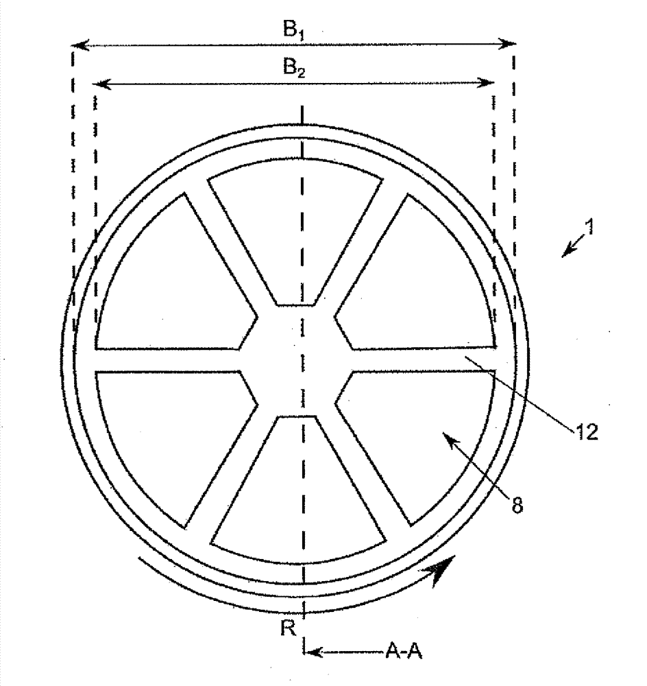
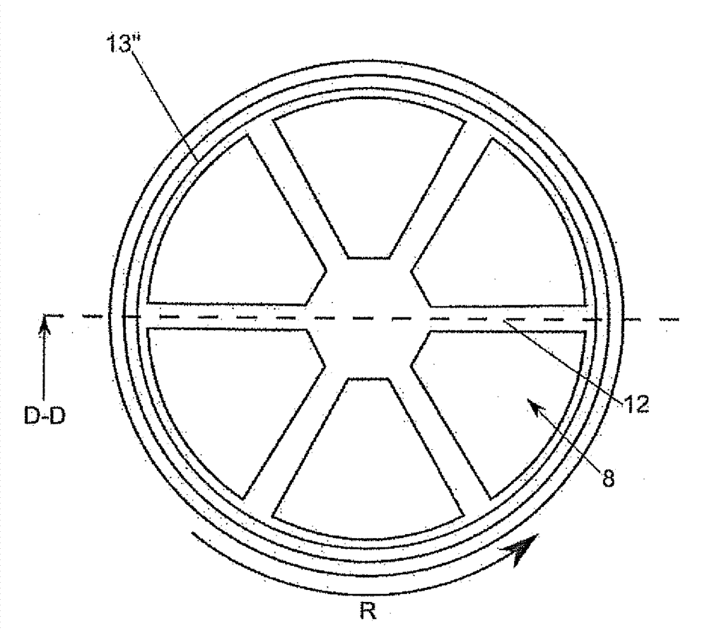
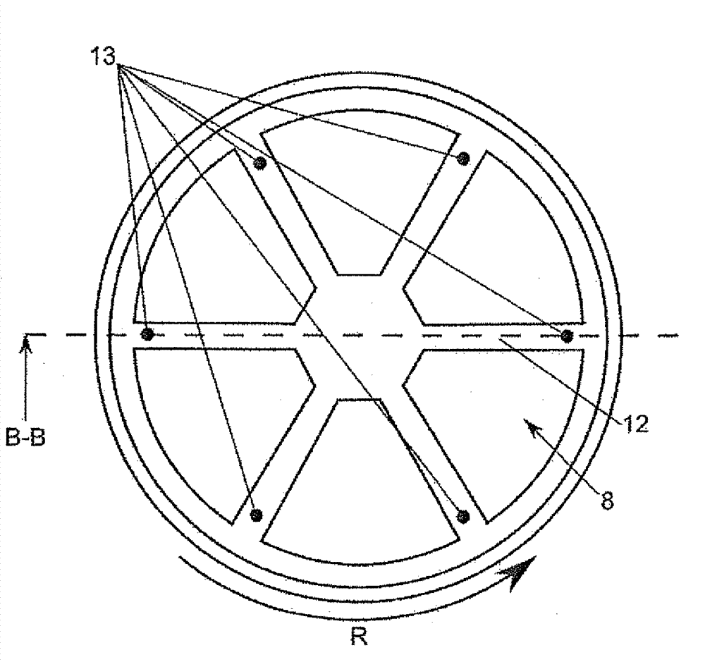
[0036] The figures show different embodiments of a receiving device 1 for receiving and mounting wafers 3 . The receiving of the wafer 3 is by means of the contact of the contact surface 3a of the wafer 3 on the mounting surface 2, 2', 2'', 2''' (for example by taking the wafer from a wafer stack or a wafer cassette not shown in the figure). 3 and place it on the robotic arm on the mounting surface 2) to take place.

[0037] At least the main annular ring section 4 has at least two planes different from each other, namely a contact plane A on which the wafer 3 is accommodated and if necessary fixed. In this process, provision can be made to touch only a part of the contact surface 3 a of the wafer 3 , particularly preferably the annular peripheral wall (contact surface between wafer 3 and receptacle 1 ).

[0038] Backside boundaries around recesses or...


PUM


Abstract

The present invention relates to an accommodating device for accommodation and mounting of a wafer (3 ) for application of a fluid (9) to a top (3o) of the wafer (3) with the following features: a revolving ring section (4) with:d) a revolving upper edge (5), e) a revolving recess (6) and f) a circumferential wall (7) running from the upper edge (5) to the recess (6), a contact plane (A) arranged within the ring section (4) for the accommodation of the wafer (3) on a contact surface (3a) of the wafer (3), wherein the ring section (4) by means of accommodation of the wafer (3) forms with said wafer an accommodating space (8) for accommodation of the fluid (9).

Description

[0001] This invention was made pursuant to a joint research agreement between Eastman Chemical Company and EV Group, Inc. in effect prior to the date the invention was made. technical field [0002] The invention relates to a receiving device for receiving and mounting a wafer for processing the wafer according to claim 1 . Background technique [0003] In the semiconductor industry, various types of containment devices, also called sample holders or chucks, are used. Depending on the respective application process, there are various sample holders, which can be heated over the entire surface or locally, and have varying forms and sizes and are based on different support principles. The most frequently used method for securing a wafer to a holder consists in creating a vacuum in a structure on the mounting surface of the holder. Often the purpose of the chuck consists inter alia of adequately securing the wafer during rotation. [0004] During some types of wafer processin...

Claims


Application Information

Patent Timeline
Patent Type & Authority Applications(China)
IPC IPC(8): H01L21/683
CPCH01L21/67046H01L21/67051H01L21/67057H01L21/68735H01L21/6704
Inventor S.霍克斯泰特勒R.D.彼得斯T.阿克拉
Owner イーヴィーグループインコーポレイテッド
Why Eureka
Try Eureka