Semiconductor memory apparatus

a memory apparatus and semiconductor technology, applied in the direction of digital storage, pulse automatic control, instruments, etc., can solve the problems of pll circuit, dll circuit not suitable for high-frequency operation, pll circuit stability deterioration in low-frequency operation, etc., and achieve excellent characteristic

Active Publication Date: 2010-09-21
SK HYNIX INC
View PDF14 Cites 22 Cited by
  • Summary
  • Abstract
  • Description
  • Claims
  • Application Information

AI Technical Summary

Problems solved by technology

However, the DLL circuit has a disadvantage in that the DLL circuit is not suitable for a high-frequency operation.
On the contrary, the PLL circuit is suitable for the high-frequency operation, but the stability of the PLL circuit deteriorates in the low-frequency operation.
Like this, in a case when the PLL circuit has the negative delay circuit, the PLL circuit has a disadvantage in that the performance thereof deteriorates.
Consequently, the semiconductor memory apparatus had a problem in that the operational stability thereof deteriorates when performing a high-speed data output operation.
As a result, the reliability of a data output operation cannot be largely secured.

Method used


Image

  • Semiconductor memory apparatus
  • Semiconductor memory apparatus
  • Semiconductor memory apparatus

Examples


Embodiment Construction

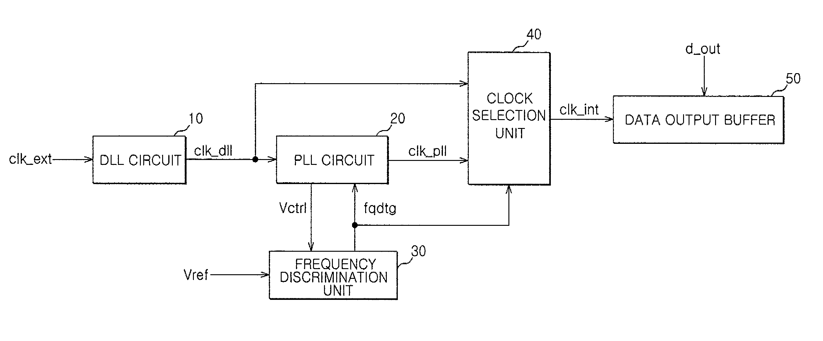
[0019]FIG. 1 is a block diagram illustrating a configuration of a semiconductor memory apparatus according to one embodiment of the invention and schematically illustrates the configuration of a circuit that generates an internal clock signal and performs a data output operation.

[0020]As shown in FIG. 1, the semiconductor memory apparatus includes a DLL circuit, 10, a PLL circuit 20, a frequency discrimination unit 30, a clock selection unit 40, and a data output buffer 50.

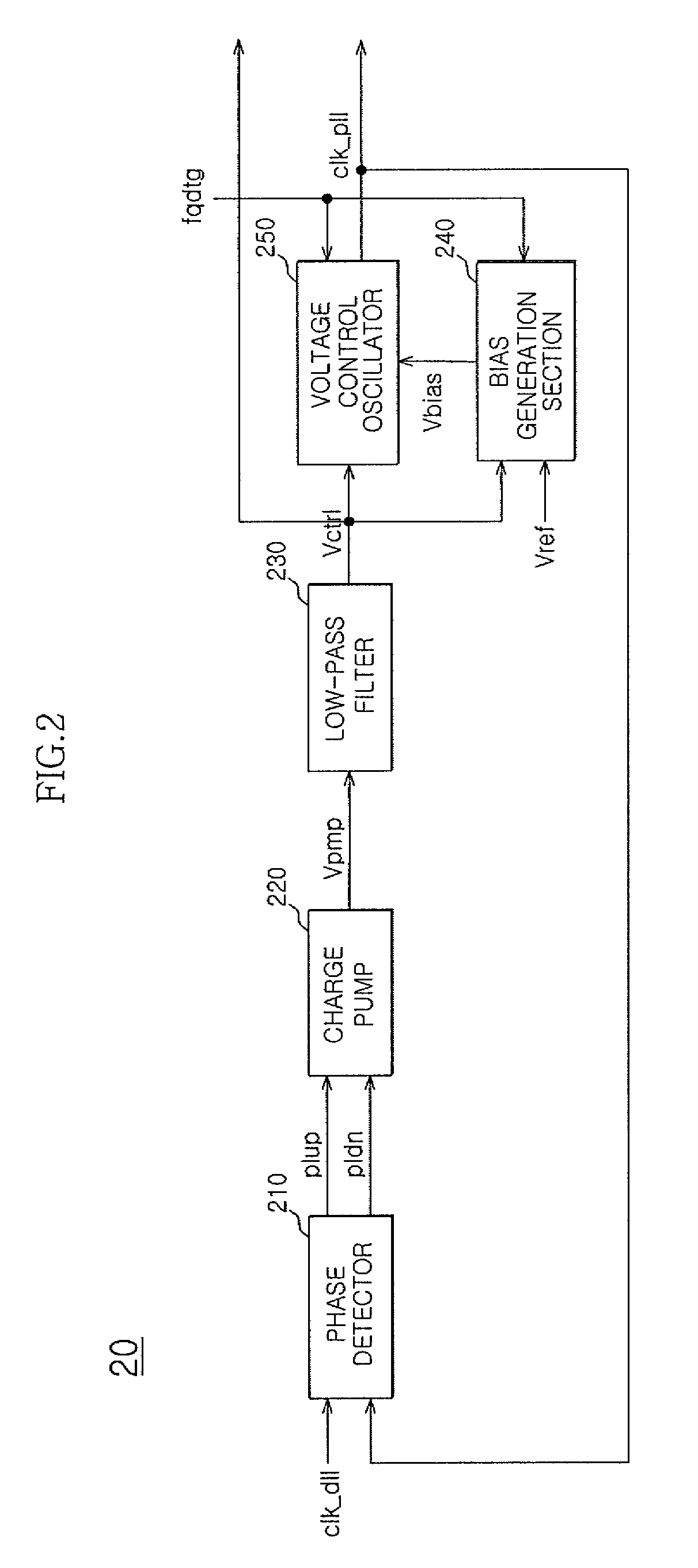
[0021]The DLL circuit 10 can negatively delay an external clock signal ‘clk_ext’ to generate a DLL clock signal ‘clk_dll’. The PLL circuit 20 can receive the DLL clock signal ‘clk_dll’, generate a control signal ‘Vctrl’ in response to a frequency of the DLL clock signal ‘clk_dll’ and generate a PLL clock signal ‘clk_pll’ having a frequency corresponding to a level of the control voltage ‘Vctrl’. The frequency discrimination unit 30 can discriminate the frequency of the DLL clock signal ‘clk_dll’ in accordance with...


PUM


Abstract

A semiconductor memory apparatus having a clock signal generation circuit and a data output circuit is presented. The apparatus includes a delay locked loop (DLL), a phase locked loop (PLL), a frequency discrimination unit, and a data output buffer. The DLL circuit is configured to negatively delay a clock signal to generate a DLL clock signal. The PLL circuit is configured to receive the DLL clock signal to generate a control voltage in response to a frequency of the DLL clock signal and to generate a PLL clock signal of a frequency corresponding to a level of the control voltage. The frequency discrimination unit is configured to discriminate a frequency of the DLL clock signal in accordance with the level of the control voltage to generate a frequency discrimination signal. The data output buffer is configured to receive the DLL clock signal or the PLL clock signal to buffer output data signals.

Description

CROSS-REFERENCES TO RELATED APPLICATION[0001]The present application claims priority under 35 U.S.C 119(a) to Korean Application No. 10-2008-0110892, filed on Nov. 10, 2008, in the Korean Intellectual Property Office, which is incorporated herein by reference in its entirety as if set forth in full.BACKGROUND[0002]1. Technical Field[0003]The embodiment described herein relates to a semiconductor memory apparatus, and more particularly, to a clock signal generation circuit and a data output circuit of a semiconductor memory apparatus.[0004]2. Related Art[0005]A conventional semiconductor memory apparatus includes a clock signal generation circuit such as a delay locked loop (DLL) circuit or a phase locked loop (PLL) circuit. The semiconductor memory apparatus has improved an operational speed thereof by synchronizing output data by means of an internal clock signal generated from the clock signal generation circuit. The DLL circuit is configured to provide a negative delay to an exte...

Claims


Application Information

Patent Timeline
Patent Type & Authority Patents(United States)
IPC IPC(8): H03L7/06
CPCH03L7/07H03L7/0995H03L7/0812H03L2207/06G11C8/00G11C7/10G11C5/14
Inventor LEE, HYUN WOOYUN, WON JOO
Owner SK HYNIX INC
Why Eureka
Try Eureka