Semiconductor memory device having duty cycle correction circuit and interpolation circuit interpolating clock signal in the semiconductor memory device

a technology of semiconductor memory and duty cycle correction circuit, which is applied in the direction of digital storage, generating/distributing signals, instruments, etc., can solve problems such as data distortion

Active Publication Date: 2005-08-23
SAMSUNG ELECTRONICS CO LTD
View PDF9 Cites 84 Cited by
  • Summary
  • Abstract
  • Description
  • Claims
  • Application Information

AI Technical Summary

Benefits of technology

[0021]Preferably, the capacitances of the first, second, and third of capacitors are controlled by CAS latency of the semiconductor memory device. When the CAS latency is high

Problems solved by technology

In synchronous semiconductor memory devices that output data by synchronizing with a clock, when the duty cycle of a clock signal is not precisely controlled distortion of the data can occur.
Ho

Method used


Image

  • Semiconductor memory device having duty cycle correction circuit and interpolation circuit interpolating clock signal in the semiconductor memory device
  • Semiconductor memory device having duty cycle correction circuit and interpolation circuit interpolating clock signal in the semiconductor memory device
  • Semiconductor memory device having duty cycle correction circuit and interpolation circuit interpolating clock signal in the semiconductor memory device

Examples


Embodiment Construction

[0032]The present invention will now be described more fully with reference to the accompanying drawings, in which preferred embodiments of the invention are shown. The same reference numerals in different drawings represent the same element.

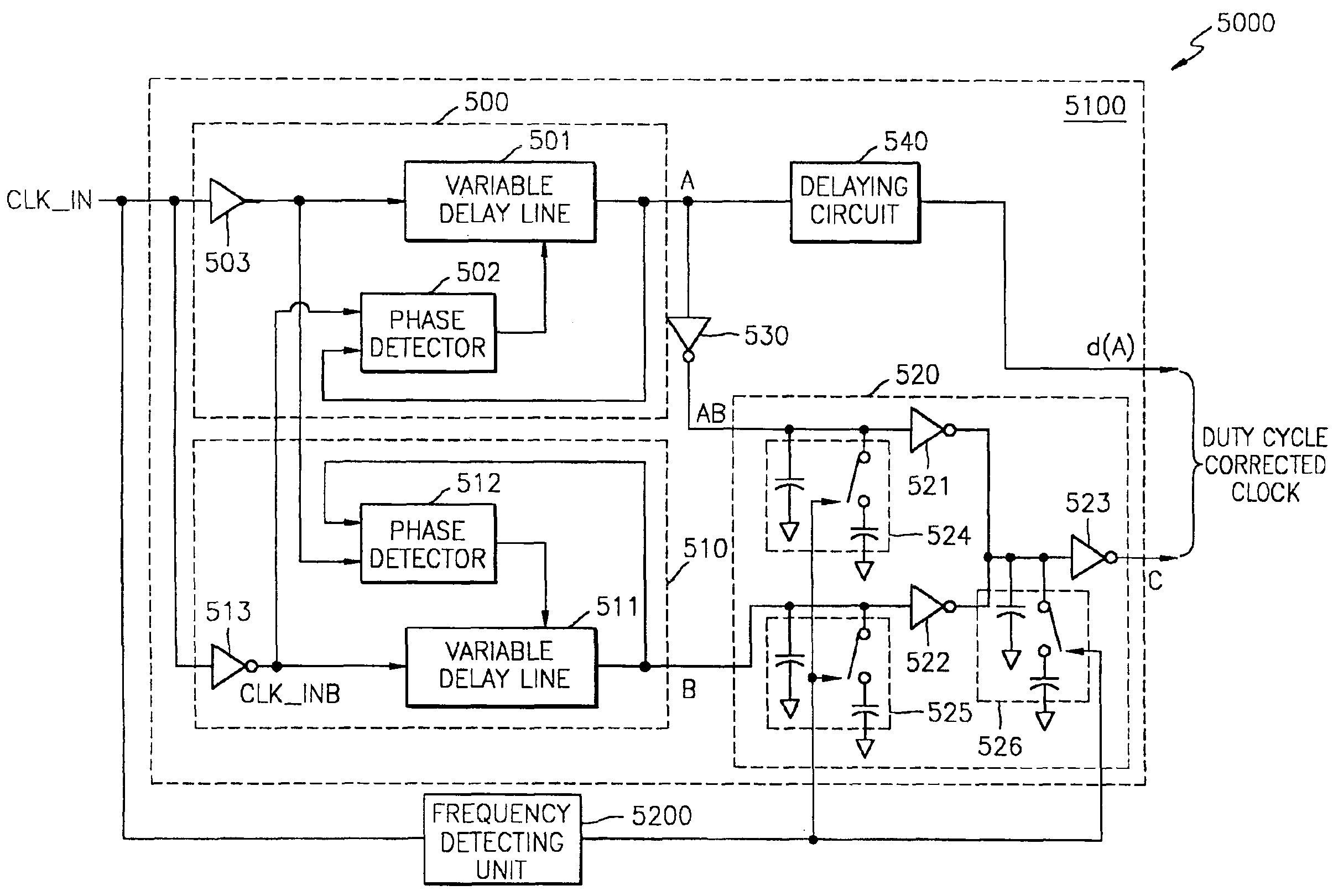
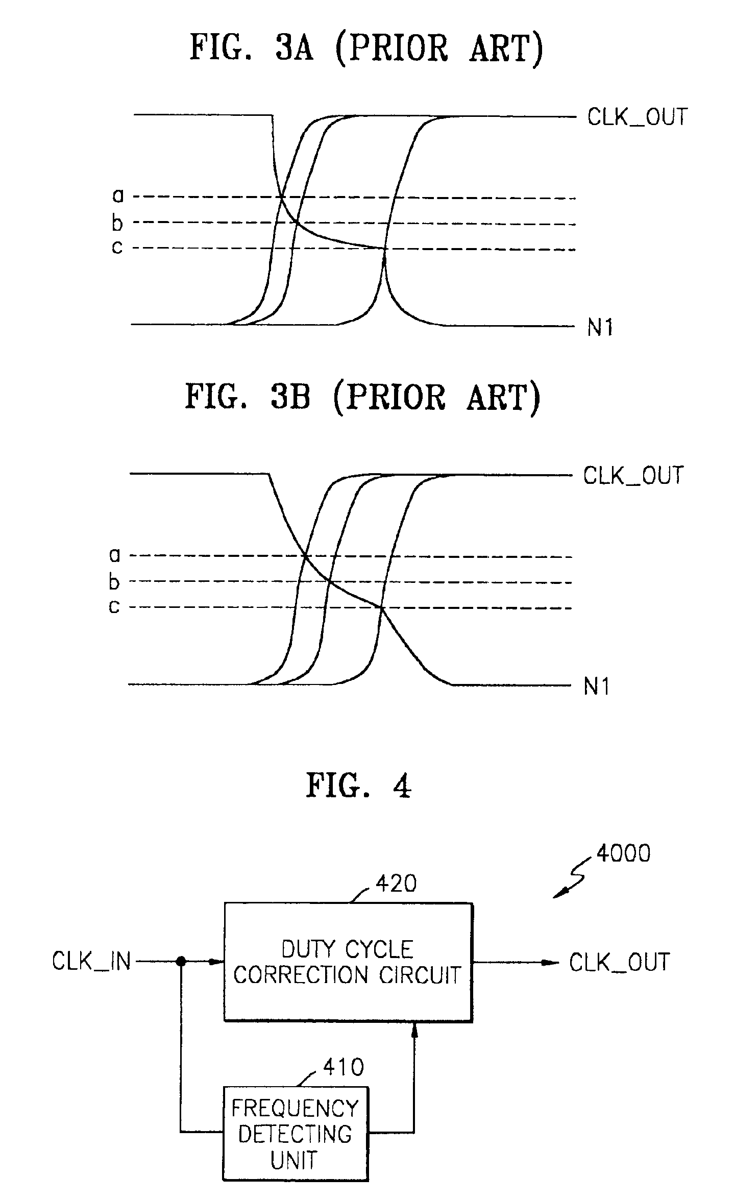
[0033]FIG. 4 is a schematic block diagram of a semiconductor memory device 4000 having a duty cycle correction circuit according to an embodiment of the present invention. The semiconductor memory device 4000 includes a frequency detecting unit 410 and a duty cycle correction circuit 420.

[0034]The frequency detecting unit 410 receives an external clock CLK_IN, detects clock frequency information of the external clock CLK_IN, and outputs the detected clock frequency information to the duty cycle correction circuit 420. The duty cycle correction circuit 420 corrects the duty cycle of the external clock CLK_IN in response to the clock frequency information and outputs a corrected clock signal CLK_OUT.

[0035]The clock frequency information of the ext...


PUM


Abstract

A semiconductor memory device having a duty cycle correction circuit and an interpolating circuit interpolating a clock signal in the semiconductor memory device are disclosed. The semiconductor memory device comprises a duty cycle correction circuit, which receives an external clock, corrects the duty cycle of the external clock, and outputs the corrected duty cycle. The duty cycle correction circuit comprises a first delay locked loop that receives the external clock, inverts the external clock, synchronizes the external clock with the inverted external clock, and outputs the synchronized clock; a second delay locked loop that receives the inverted external clock, synchronizes the inverted external clock with the external clock and outputs the synchronized clock; an inverting circuit that inverts the output signal of the first delay locked loop; an interpolation circuit that interpolates the output signal of the inverting circuit with the output signal of the second delay locked loop, and outputs the interpolated signal; and a control circuit that controls the interpolation circuit in response to the clock frequency information of the external clock.

Description

BACKGROUND OF THE INVENTION[0001]This application claims priority to Korean Patent Application No. 2002-53327 filed on Sep. 4, 2002, in the Korean Intellectual Property Office, the disclosure of which is incorporated herein in its entirety by reference.[0002]1. Field of the Invention[0003]The present invention relates to a synchronous semiconductor memory device, and more particularly, to a semiconductor memory device having a duty cycle correction circuit correcting the duty cycle of an external clock signal and an interpolation circuit interpolating the clock signal in the semiconductor memory device.[0004]2. Description of the Related Art[0005]The duty cycle of a clock signal is a numerical value representing the ratio of a pulse width with respect to a pulse period of the clock signal. In digital clock applications, it is very important for the duty cycle of a clock signal to be precisely controlled. In synchronous semiconductor memory devices that output data by synchronizing w...

Claims


Application Information

Patent Timeline
IPC IPC(8): G11C7/00G11C7/22G06F1/04G06F1/10G11C11/40G11C11/407H03K5/05H03K5/156
CPCG11C7/22H03K5/1565G11C7/222G11C11/40
Inventor CHUNG, HOE-JUKIM, KYU-HYOUN
Owner SAMSUNG ELECTRONICS CO LTD
Why Eureka
Try Eureka