Display device with touch panel

a display device and touch panel technology, applied in the field of display devices with touch panels, can solve the problem of inability to increase resolution, and achieve the effect of detecting small inter-electrode capacitance and canceling parasitic capacitan

Active Publication Date: 2013-05-28
JAPAN DISPLAY INC
View PDF15 Cites 21 Cited by
  • Summary
  • Abstract
  • Description
  • Claims
  • Application Information

AI Technical Summary

Benefits of technology

[0009]The present invention has been devised in order to solve the problem in the related art and it is an object of the present invention to make it possible to cancel parasitic capacitance, detect smaller inter-electrode capacitance, and provide a high-resolution touch panel having a larger number of electrodes.
[0013]An effect obtained by representative ones among the inventions disclosed in this application is that, according to the present invention, it is possible to cancel parasitic capacitance, detect smaller inter-electrode capacitance, and provide a high-resolution touch panel having a larger number of electrodes.

Problems solved by technology

Therefore, resolution cannot be increased.

Method used


Image

  • Display device with touch panel
  • Display device with touch panel
  • Display device with touch panel

Examples


first embodiment

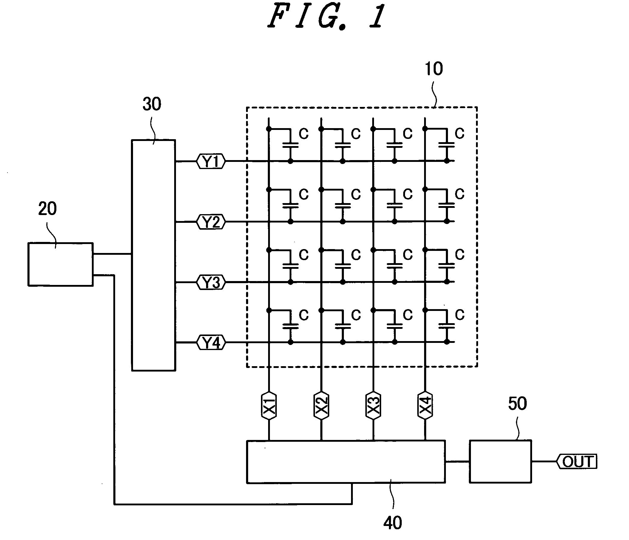
[0031]FIG. 1 is a block diagram showing the schematic structure of a touch panel used in a liquid crystal display device according to a first embodiment of the present invention.

[0032]In FIG. 1, reference numeral 10 denotes a touch sensor, 20 denotes a control circuit, 30 denotes a Y driving circuit, 40 denotes an X detection circuit, and 50 denotes a coordinate detection circuit. X1 to X4 denote X electrodes extending in a first direction (a Y direction in FIG. 1), Y1 to Y4 denote Y electrodes extending in a second direction (an X direction in FIG. 1), and C denotes coupling capacitors formed between the respective X electrodes and the respective Y electrodes.

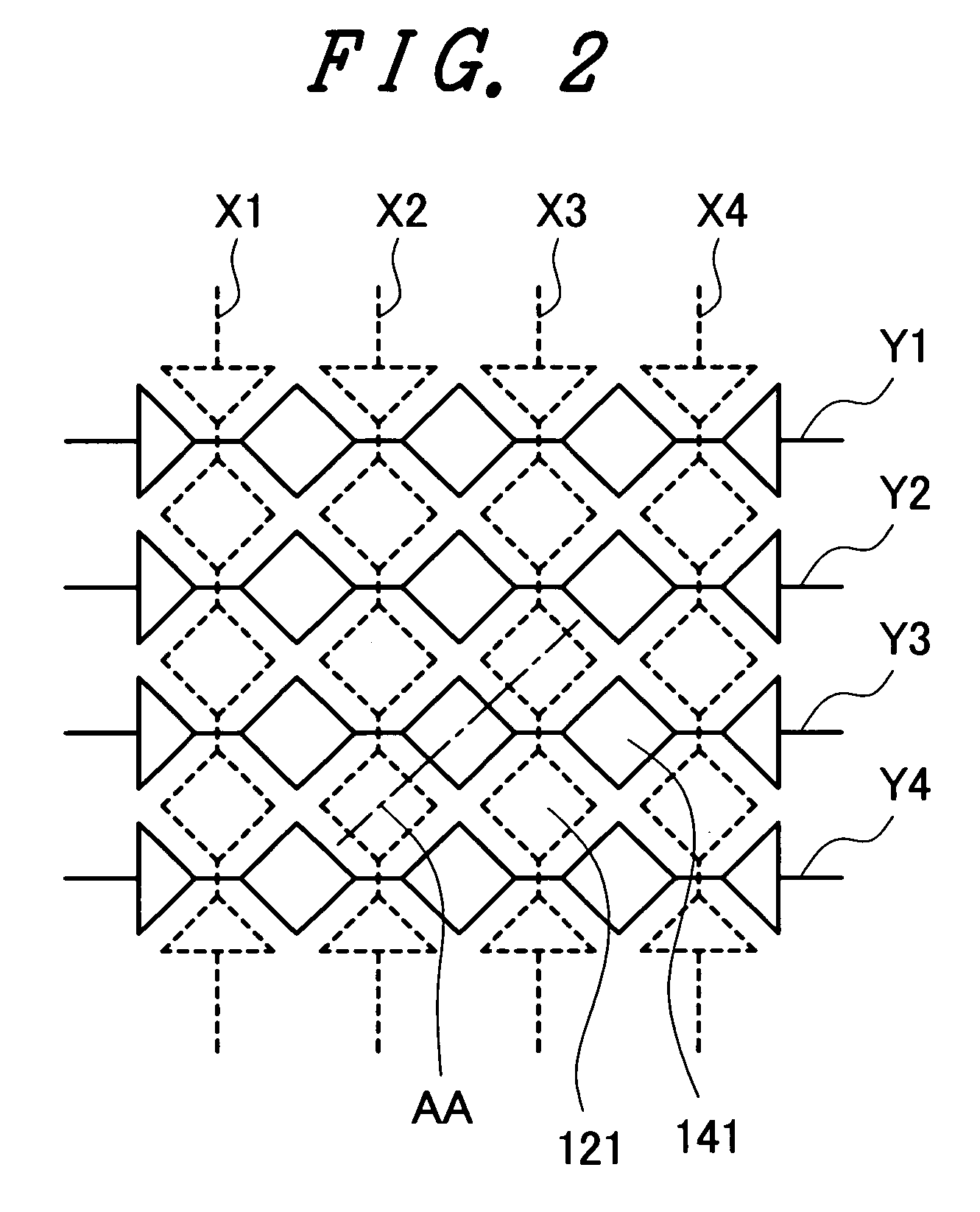
[0033]FIG. 2 is a diagram showing electrode shapes of the X electrodes and the Y electrodes shown in FIG. 1. As shown in FIG. 2, the X electrodes X1 to X4 have wide electrode patterns 121 among the Y electrodes Y1 to Y4. The Y electrodes Y1 to Y4 have wide electrode patterns 141 among the X electrodes X1 to X4.

[0034]FIG. 3 is ...

second embodiment

[0056]FIG. 8 is a block diagram showing the schematic structure of a touch panel used in a liquid crystal display device according to a second embodiment of the present invention.

[0057]In FIG. 8, reference numeral 10 denotes a touch sensor, 20 denotes a control circuit, 70 denotes a current detection circuit, and 80 denotes an electrode driving circuit.

[0058]In the first embodiment, the L level voltage is sequentially supplied to the respective Y electrodes in a time division manner and electric currents flowing to the respective X electrodes are detected to detect a coordinate position However, in the second embodiment, the control circuit 20 controls a switch 90 and, in a period A, the electrode driving circuit 80 sequentially supplies the L level voltage to the respective Y electrodes in a time division manner and the current detection circuit 70 detects electric currents flowing to all X electrodes and, in a period B, the electrode driving circuit 80 sequentially supplies the L ...

third embodiment

[0065]FIG. 11 is a block diagram showing the schematic structure of a touch panel used in a liquid crystal display device according to a third embodiment of the present invention.

[0066]In FIG. 11, reference numeral 10 denotes a touch sensor, 210 denotes a Y electrode selection circuit, 220 denotes an X electrode selection circuit, and 230 denotes a current detection circuit. The Y electrode selection circuit 210 and the X electrode selection circuit 220 have identical circuit configurations. However, in FIG. 11, only the circuit configuration of the Y electrode selection circuit 210 is shown.

[0067]The Y electrode selection circuit 210 and the X electrode selection circuit 220 have a scanning circuit 211 and a scanning circuit 212. The scanning circuit 212 turns off all switching elements SW3 in the period A and turns on all the switching elements SW3 in the period B.

[0068]The scanning circuit 211 sequentially controls, in a time division manner, ON and OFF of a switching element SW1...


PUM


Abstract

A touch panel includes plural first electrodes extending in a first direction, plural second electrodes extending in a second direction different from the first direction, a driving circuit, a detection circuit, and a coordinate-position calculating circuit. The driving circuit sequentially selects two first electrodes out of the plural first electrodes, supplies a high potential voltage higher than a reference voltage to one of the selected two first electrodes, and supplies the reference voltage to the other, the detection circuit detects a capacitance difference (A−B) between a capacitor A between a selected one of the second electrodes and the first electrode to which the high potential voltage is supplied and a capacitor B between the selected second electrode and the first electrode to which the reference voltage is supplied, and the coordinate-position calculating circuit calculates a touch position on the touch panel touched by the observer on the basis of positions of the selected first and second electrodes and the capacitance difference (A−B).

Description

[0001]The present application claims priority from Japanese applications JP2007-175050 filed on Jul. 3, 2007, the content of which is hereby incorporated by reference into this application.BACKGROUND OF THE INVENTION[0002]1. Field of the Invention[0003]The present invention relates to a display device with touch panel, and, more particularly to a display device with touch panel having an electrostatic capacitance coupling type touch panel function that is capable of detecting plural touch positions touched by an observer.[0004]2. Description of Related Art[0005]In recent years, according to the spread of mobile apparatuses, a touch panel technique for supporting a “user friendly” graphical user interface is becoming important.[0006]As the touch panel technique, an electrostatic capacitance coupling type touch panel is known. As the electrostatic capacitance coupling type touch panel, a touch panel that detects plural touch positions touched by an observer is known (see JP-A-8-16307)...

Claims


Application Information

Patent Timeline
Patent Type & Authority Patents(United States)
IPC IPC(8): G06F3/041
CPCG02F1/13338G06F3/0416G06F3/044G06F3/04166G06F3/0445G06F3/0446G06F3/0412
Inventor SATO, HIDEONISHITANI, SHIGEYUKISAITO, TERUAKI
Owner JAPAN DISPLAY INC
Why Eureka
Try Eureka