Eeprom with split gate source side injection

a technology of source side injection and eeprom, which is applied in the direction of transistors, solid-state devices, instruments, etc., can solve the problems of difficult to pit the substrate without pitting, severe junction leakage as well as loss of a portion of the bn+ conductor, and additional process complexity of forming the thin oxide region and extra space needed to place this thin oxide region

Inactive Publication Date: 2004-04-01
SANDISK TECH LLC
View PDF81 Cites 22 Cited by
  • Summary
  • Abstract
  • Description
  • Claims
  • Application Information

AI Technical Summary

Problems solved by technology

This is difficult to do without pitting the substrate as well as the exposed BN+ when etching the exposed poly 1 between adjacent cells.
This is actually forming trench isolation, but with BN+ abutting this trench, we may experience severe junction leakage as well as loss of a portion of the BN+ conductor.
However, there is the a...

Method used


Image

  • Eeprom with split gate source side injection
  • Eeprom with split gate source side injection
  • Eeprom with split gate source side injection

Examples


first embodiment

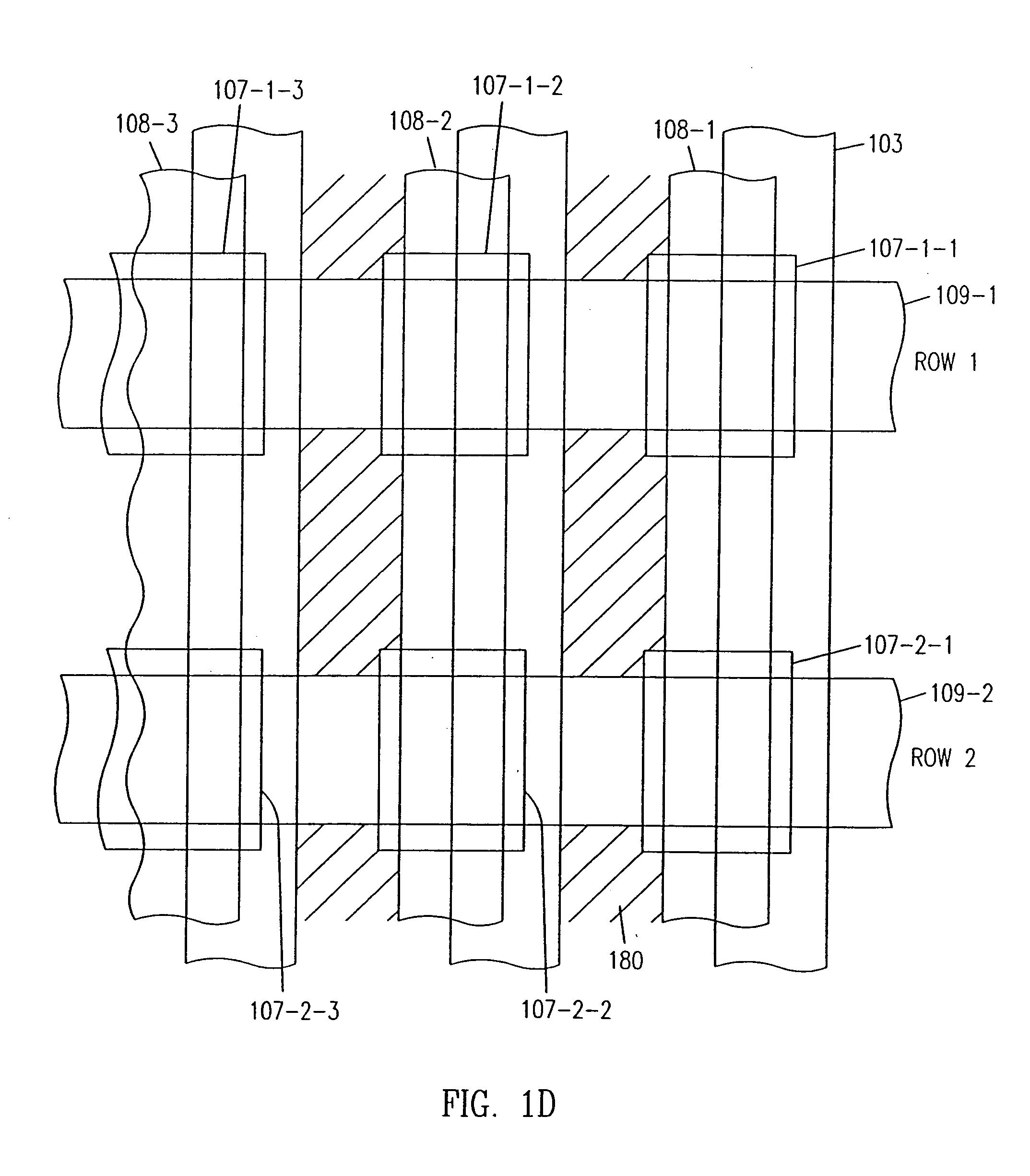
[0098] A second array embodiment is similar to that of FIG. 1d but uses the cell embodiment shown in FIG. 1b, to form a row oriented sector architecture, is shown in FIG. 1g. A sector consists of a group of rows, four in this example, which are erased together. Erase uses option 2 of Table 1, for this row oriented sector architecture, bringing all the poly 3 word lines of a sector to high voltage. The poly 2 steering gate is common to a group of N sectors where N can range from 1 to the full size of the memory array. Similarly the BN+ columns can alternatively continuously span the full length of the array or be broken down into a collection of shorter length, local columns. These connect to a global (full array length) column through a select transistor driven by an additional level of decoding. The local columns can range from 1 to N sectors. The preferred embodiment is to have local columns span the same number of sectors as the poly 2 steering gate. A preferred number of sectors...

second embodiment

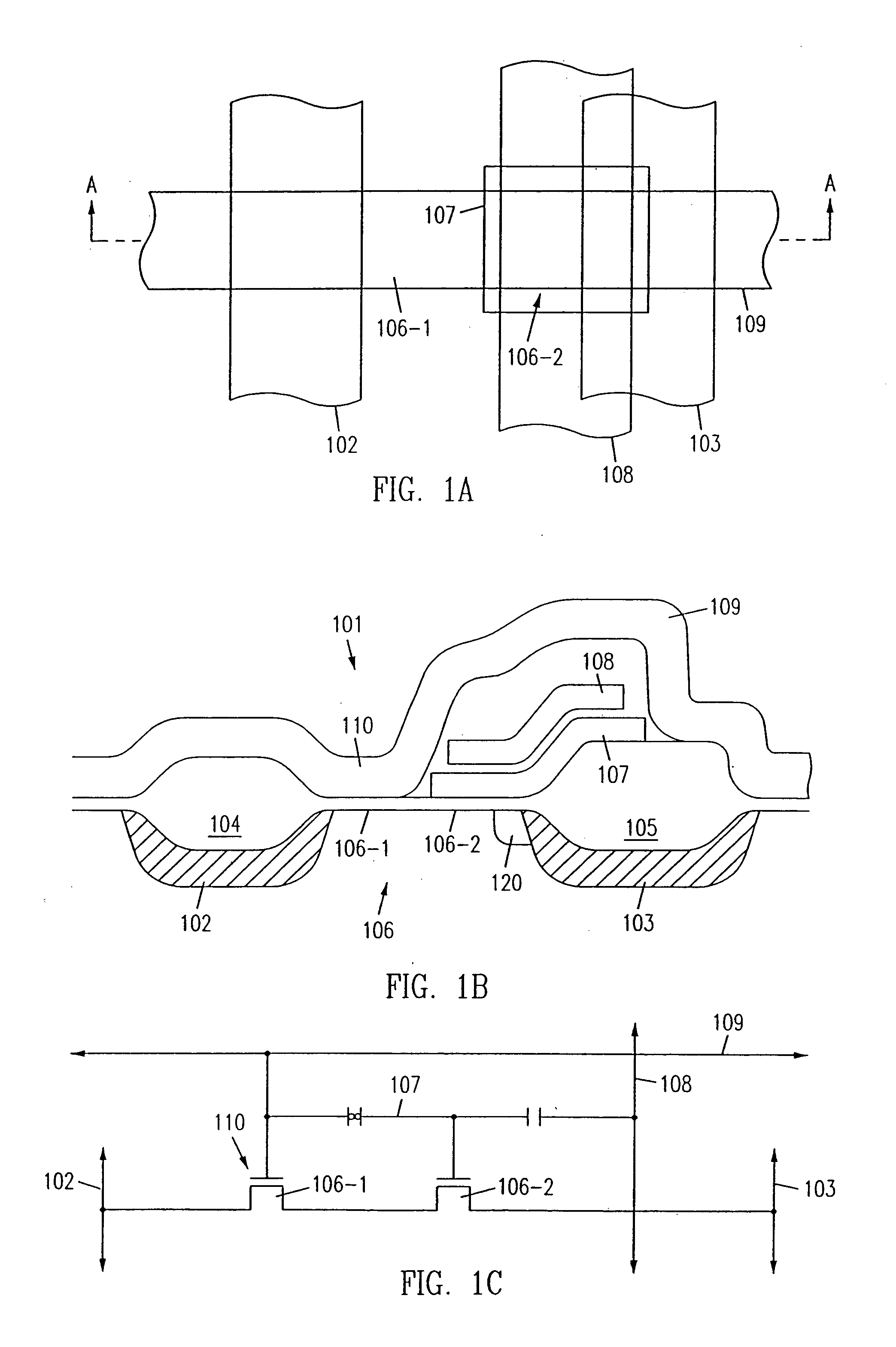
[0108] FIG. 5 is a two-poly embodiment in which programming occurs by taking drain 303 high, for example about 10V while raising control gate 308 just sufficiently so as to turn on select transistor 310. Since this V.sub.CG voltage can vary from one device to another it is possible to achieve the optimum injection conditions by keeping V.sub.CG at about 3V while raising source (virtual ground) 302 in a sawtooth fashion from about 0 to 3 volts and back to 0 again, with a period on the order approximately 1 microsecond.

[0109] This ensures that at some point along the sawtooth the optimum injection conditions are met. Reference can also be made to European Patent Application Serial No. 89312799.3 filed Aug. 12, 1989. To further enhance programming efficiency, in one embodiment a programming efficiency implant 330 (shown in dotted line) is introduced at the source side. To read the device, its source is 0V, drain is approximately 1.0 v and V.sub.CG approximately 4.5-5 v. To erase we emp...

third embodiment

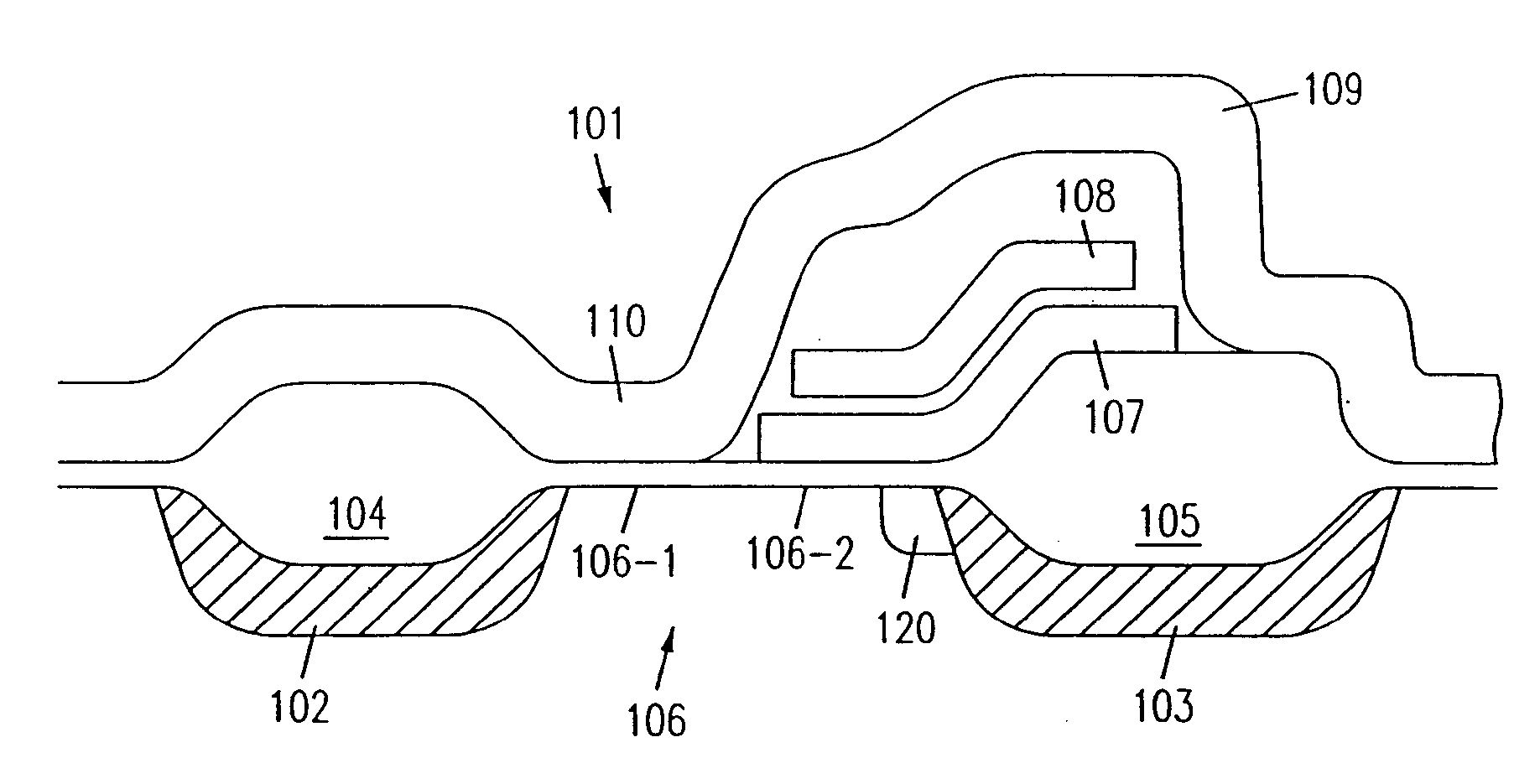
[0118] FIG. 6 is a cross-sectional view of alternative embodiment of a two poly cell, using source side injection for programming, aided by strong coupling to buried N+ drain 403, which acts also as a second control gate. Erase is by Fowler-Nordheim tunneling to channel 406 through a small thinned oxide region, formed for example to a thickness of about 100 .ANG., by utilizing a thin polyspacer. These process steps would be as follows: Once the drain oxide is formed (i.e. the oxide above drain 403), a first layer of poly, (approximately 2000 .ANG. to 4000 .ANG. thick) is deposited and a thin nitride dielectric is deposited on top. These layers are then etched using a poly 1 mask to delineate the lateral extent (as shown in FIG. 6) of the poly 1. A second layer of nitride is then deposited and anistropically etched back to underlying oxide, leaving the initial nitride layer on top of poly 1 plus nitride spacers along the poly 1 sidewalls. This protects the poly 1 sidewall from subseq...


PUM


Abstract

Novel memory cells utilize source-side injection, allowing very small programming currents. If desired, to-be-programmed cells are programmed simultaneously while not requiring an unacceptably large programming current for any given programming operation. In one embodiment, memory arrays are organized in sectors with each sector being formed of a single column or a group of columns having their control gates connected in common. In one embodiment, a high speed shift register is used in place of a row decoder to serially shift in data for the word lines, with all data for each word line of a sector being contained in the shift register on completion of its serial loading. In one embodiment, speed is improved by utilizing a parallel loaded buffer register which receives parallel data from the high speed shift register and holds that data during the write operation, allowing the shift register to receive serial loaded data during the write operation for use in a subsequent write operation. In one embodiment, a verification is performed in parallel on all to-be-programmed cells in a column and the bit line current monitored. If all of the to-be-programmed cells have been properly programmed, the bit line current will be substantially zero. If bit line current is detected, another write operation is performed on all cells of the sector, and another verify operation is performed. This write/verify procedure is repeated until verification is successful, as detected or substantially zero, bit line current.

Description

[0001] This application is a continuation-in-part of U.S. Ser. No. 08 / 193,707 filed Feb. 9, 1994, which in turn is a divisional of U.S. Ser. No. 07 / 820,364, filed Jan. 14, 1992, now U.S. Pat. No. 5,313,421 issued May 17, 1994.[0002] This invention pertains to semiconductor memory cells and arrays, more particularly to electrically erasable programmable read only memories.[0003] Erasable programmable read only memories (EPROMs) and electrically erasable programmable read only (EEPROMs) are well known in the art. These devices have the ability to store data in non-volatile fashion, while also being capable of being erased and rewritten as desired. EPROM devices are typically erased by exposing the integrated circuit device to ultraviolet radiation, while EEPROMs allow erasure to be performed electrically.[0004] One form of EEPROM device includes a so-called "split-gate" electrode, in which the control gate includes a first portion overlaying a floating gate and a second portion direct...

Claims


Application Information

Patent Timeline
IPC IPC(8): G11C7/00G11C16/00G11C16/04H01L21/336H01L21/8247H01L27/115H01L29/76H01L29/788H01L31/107H01L33/00
CPCG11C16/0425G11C16/0458H01L29/7881H01L27/115H01L27/11521G11C16/0491H10B69/00H10B41/30
Inventor GUTERMAN, DANIEL C.SAMACHISA, GHEORGHEFONG, YUPIN KAWINGHARARI, ELIYAHOU
Owner SANDISK TECH LLC
Why Eureka
Try Eureka