Sense amplifier circuit and semiconductor device

a technology of amplifier circuit and semiconductor device, which is applied in the direction of information storage, static storage, digital storage, etc., can solve the problems of difficult configuration application, difficulty in obtaining a sufficient capacitance value of a capacitor included in a memory cell for the purpose of miniaturization of the memory cell, etc., and achieve excellent operating margin, high-speed reading, and high-speed reading

Active Publication Date: 2011-03-17
LONGITUDE LICENSING LTD
View PDF5 Cites 18 Cited by
  • Summary
  • Abstract
  • Description
  • Claims
  • Application Information

AI Technical Summary

Benefits of technology

In addition, by overdriving the gate voltage of the first MOS transistor, an operation of driving the bit line to the predetermined voltage can be performed in a short time before the sensing operation, and thus high-speed reading can be achieved.
Meanwhile, by previously driving the bit line to the predetermined voltage using the first precharge circuit, the sensing operation can be performed in a short time, and thus high-speed reading can be achieved.
Further, in a semiconductor device having a hierarchical bit line structure and a hierarchical sense amplifier circuit, the capacitance at each local bit line can be set to a small value, and therefore excellent operating margin can be obtained in the large capacity semiconductor device.
Furthermore, fluctuation of the threshold voltage of the MOS transistor due to manufacturing process and temperature can be appropriately compensated by using the compensated voltage generating circuit. Therefore, the operating margin for sensing can be further improved, thereby improving reliability of the operation of the sense amplifier circuit. Or, since the variation permissible range in the chip can be expanded, when large number of sense amplifier circuits can be implemented in a large capacity DRAM using memory cells each having a small capacitance, it is possible to improve production yield and to reduce manufacturing cost.

Problems solved by technology

As capacity of semiconductor memory devices such as a DRAM has recently become large, it has become difficult to obtain a sufficient capacitance value of a capacitor included in a memory cell for the purpose of miniaturization of the memory cell.
As described above, the conventional charge transfer type sense amplifier circuit has a problem in that it is difficult to apply to the configuration achieving the lower voltage operation using memory cells MC having a small capacitance.

Method used


Image

  • Sense amplifier circuit and semiconductor device
  • Sense amplifier circuit and semiconductor device
  • Sense amplifier circuit and semiconductor device

Examples


first embodiment

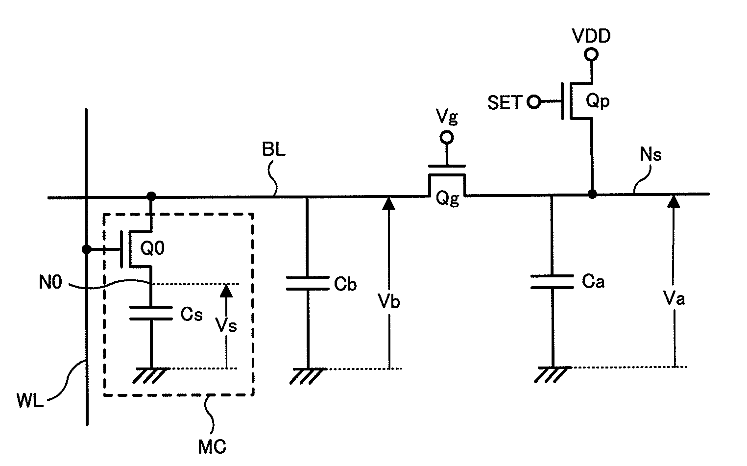
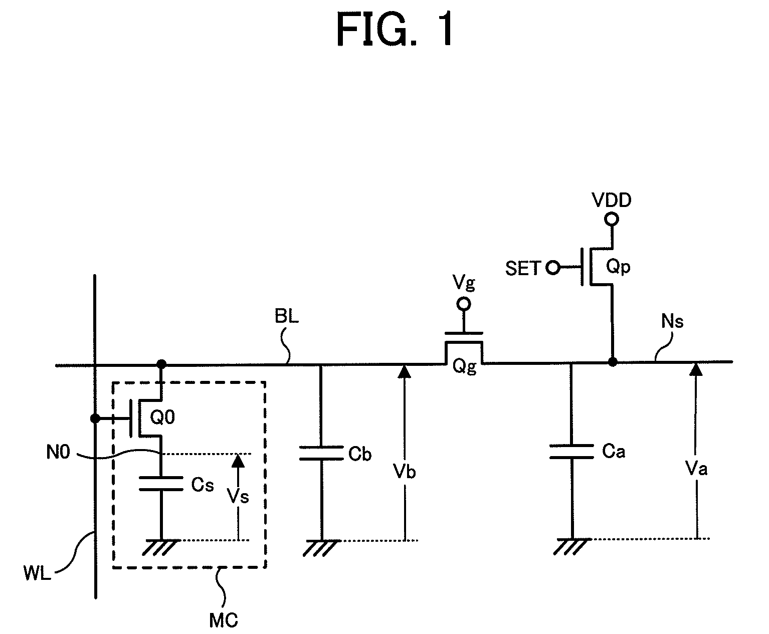
A first embodiment of the invention will be described below. A feature of the first embodiment is that a single-ended sense amplifier circuit controlled in the charge transfer mode and the charge distributing mode is employed. FIG. 3 shows a configuration example of a sensing part in a DRAM of the first embodiment, in which a memory cell MC, a preamplifier 10 functioning as the above basic operation of the sense amplifier circuit, and a sense latch circuit 11 located subsequent to the preamplifier 10 are shown.

The memory cell MC is a 1T1C type DRAM memory cell composed of an N-type MOS selection transistor Q0, and a capacitor Cs storing information as electric charge. The selection transistor Q0 has a source connected to the bit line BL and a gate connected to the word line WL. The capacitor Cs is connected between the drain of the selection transistor Q0 and a cell plate voltage VPLT. Although FIG. 3 shows one memory cell MC, a large number of memory cells MC arranged at intersecti...

second embodiment

Next, a second embodiment of the invention will be described. In the second embodiment, a hierarchical memory cell array is formed, and the charge transfer / distributing type single-ended sense amplifier of the first embodiment is applied to a DRAM having hierarchical bit lines and hierarchical sense amplifier circuits. FIG. 8 shows a configuration example of a sensing part in the DRAM of the second embodiment, in which a memory cell MC, a local bit line LBL and a global bit line GBL which serve as the hierarchical bit lines, and a local sense amplifier 20 and a global sense amplifier 21 which serve as the hierarchical sense amplifier circuits are respectively shown. The local bit line LBL connected to the memory cell MC is selectively connected to the global bit line GBL via the local sense amplifier 20, and data thereof is transmitted to the corresponding global sense amplifier 21. Although FIG. 8 shows only part of the configuration, the second embodiment employs the configuration...

third embodiment

Next, a third embodiment of the invention will be described. In a DRAM of the third embodiment, hierarchical bit lines and hierarchical sense amplifier circuits are configured in the same manner as the second embodiment, part of which differs from the second embodiment. Although the circuit configuration in FIG. 9 of the second embodiment is almost common to the third embodiment, a configuration of certain power source circuits is modified. That is, a compensated voltage generating circuit which compensates fluctuation of the threshold voltage Vt1 of the MOS transistor Q1 and a compensated voltage generating circuit which compensates fluctuation of the threshold voltage Vt2 of the MOS transistor Q2 are employed. Specific configurations thereof will be described below.

FIG. 13 shows an example of a circuit configuration of the global sense amplifier 21 of the third embodiment. The basic circuit configuration in FIG. 13 is almost common to FIG. 9 of the second embodiment, in which howe...


PUM


Abstract

A single-ended sense amplifier circuit of the invention comprises first and second MOS transistors and first and second precharge circuits. The first MOS transistor drives the bit line to a predetermined voltage and switches connection between the bit line and a sense node and the second MOS transistor whose gate is connected to the sense node amplifies the signal via the first MOS transistor. The first precharge circuit precharges the bit line to a first potential and the second precharge circuit precharges the sense node to a second potential. Before sensing operation, the bit line is driven to the predetermined voltage when the above gate voltage is controlled to decrease. The predetermined voltage is appropriately set so that a required voltage difference at the sense node between high and low levels can be obtained near a changing point between charge transfer/distributing modes.

Description

BACKGROUND OF THE INVENTION1. Field of the InventionThe present invention relates to a single-ended sense amplifier circuit amplifying a signal read out from a memory cell and transmitted through a bit line, and to a semiconductor device having the single-ended amplifier circuit.2. Description of Related ArtAs capacity of semiconductor memory devices such as a DRAM has recently become large, it has become difficult to obtain a sufficient capacitance value of a capacitor included in a memory cell for the purpose of miniaturization of the memory cell. A charge transfer type sense amplifier circuit is conventionally known as a sense amplifier circuit suitable for amplifying a minute signal voltage read out from the memory cell. For example, configurations of a variety of charge transfer type sense amplifiers are disclosed in the following Patent References 1 to 4.Patent Reference 1: Japanese Patent Application Laid-open No. 2000-195268Patent Reference 2: Japanese Patent Application Lai...

Claims


Application Information

Patent Timeline
Patent Type & Authority Applications(United States)
IPC IPC(8): G11C11/24G11C7/06
CPCG11C7/065G11C7/067G11C7/1087G11C7/06G11C5/147G11C11/4091
Inventor KAJIGAYA, KAZUHIKOYOSHIDA, SOICHIROYAMADA, YASUTOSHI
Owner LONGITUDE LICENSING LTD
Why Eureka
Try Eureka