
Nonvolatile semiconductor memory and its drive method
A non-volatile, semiconductor technology, applied in semiconductor devices, semiconductor/solid-state device manufacturing, read-only memory, etc., can solve problems such as difficult injection of charges, and achieve high-speed reading effects
- Summary
- Abstract
- Description
- Claims
- Application Information
AI Technical Summary
Problems solved by technology
Method used
Image

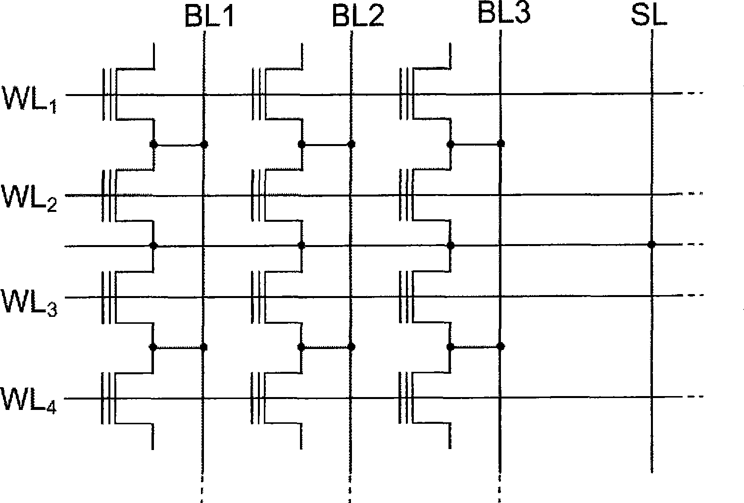
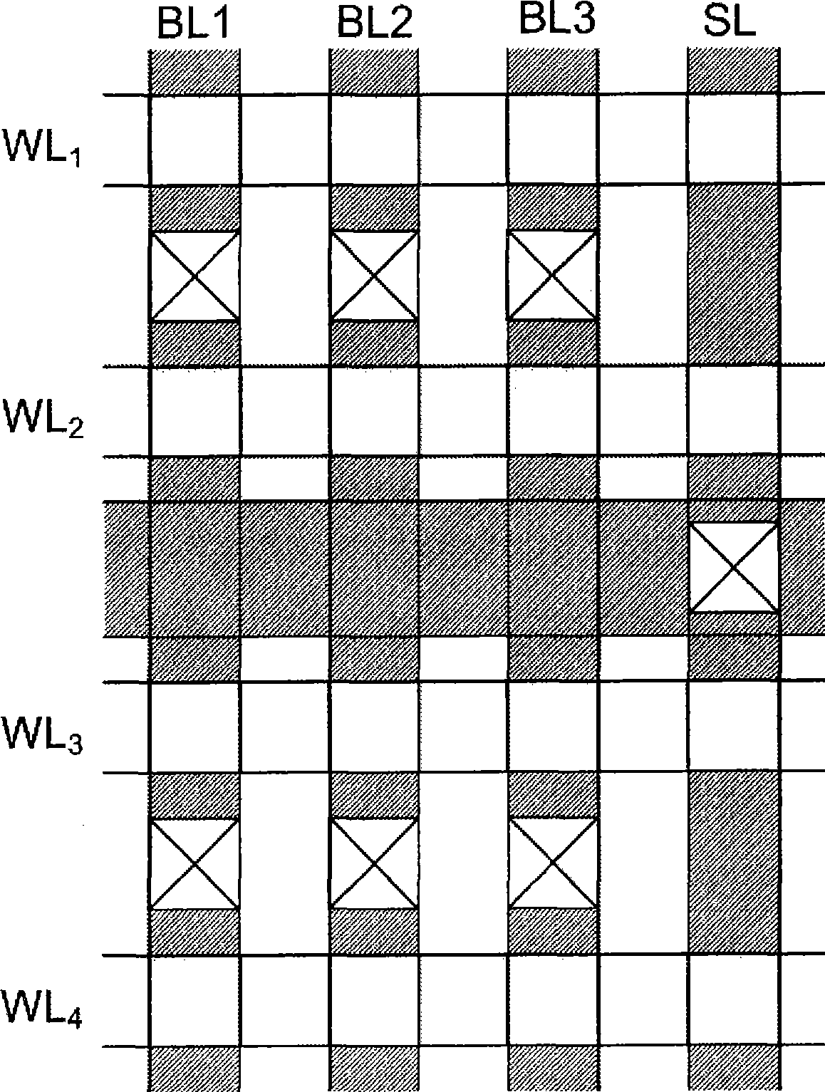
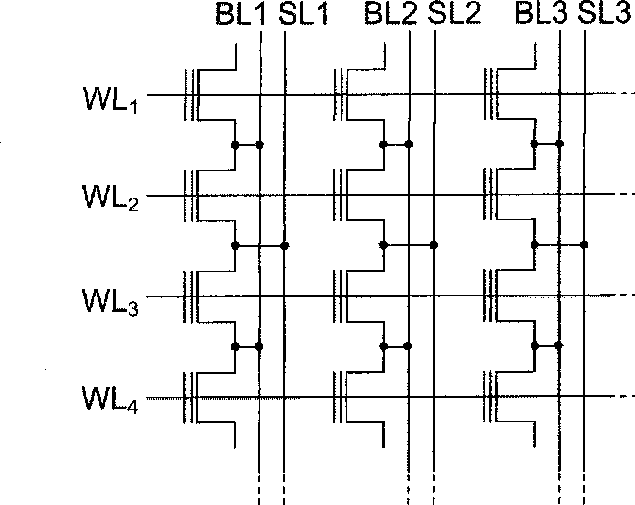
Examples
Embodiment
[0113] Hereinafter, the present invention will be described based on the embodiments shown in the drawings. In addition, the present invention is not limited thereto.
[0114] Figure 5 , Image 6 , Figure 7 , Figure 8 The layout and cross-sectional structure of the nonvolatile semiconductor memory according to the present invention are shown respectively. In this embodiment, the source line 2 and the source diffusion layer 3 are formed on the silicon oxide film 1, the island-shaped semiconductor layer 4 is formed thereon, and the drain diffusion layer 5 is formed on the top of the island-shaped semiconductor layer 4. A charge storage layer 6 formed of a gate insulating film is formed on the channel region of the side wall sandwiched by the drain diffusion layer 5 and the source diffusion layer 3, and the control gate 7 is formed on the charge storage layer 6, thereby forming storage unit. In addition, an island-shaped semiconductor layer 9 is formed on the source line...
PUM
 Abstract
Description
Claims
Application Information