Solid-state imaging device, method for producing solid-state imaging device, and electronic apparatus

a solid-state imaging and imaging device technology, applied in the direction of semiconductor/solid-state device details, radio frequency control devices, television systems, etc., can solve the problem of difficult high-speed transfer, suppress white flaws and another deterioration of pixel characteristics, and reduce the difficulty of high-speed reading.

Active Publication Date: 2017-06-08
BRILLNICS JAPAN
View PDF10 Cites 11 Cited by
  • Summary
  • Abstract
  • Description
  • Claims
  • Application Information

AI Technical Summary

Benefits of technology

[0031]According to the present invention, high speed reading becomes possible using a small chip area. In addition, there is little restriction in layout, and it becomes possible to suppress white flaws and another deterioration of pixel characteristics. Further, according to the present invention, it becomes possible to form a pixel portion by a CCD process having a good dark current characteristic. Further, miniaturization of pixels for global shutter becomes possible. Further, according to the present invention, a drive interface can be simplified. Further, it is also possible to eliminate the horizontal CCD, therefore reduction of the consumed power becomes possible. Further, according to the present invention, increase of functions such as digital output conversion and on-chip signal processing becomes possible.

Problems solved by technology

This IT type CCD image sensor 1 has a structure enabling progressive reading (progressive scanning), but transfers the signal charges by the horizontal CCD 3, so high speed transfer is difficult.

Method used


Image

  • Solid-state imaging device, method for producing solid-state imaging device, and electronic apparatus
  • Solid-state imaging device, method for producing solid-state imaging device, and electronic apparatus
  • Solid-state imaging device, method for producing solid-state imaging device, and electronic apparatus

Examples


first embodiment

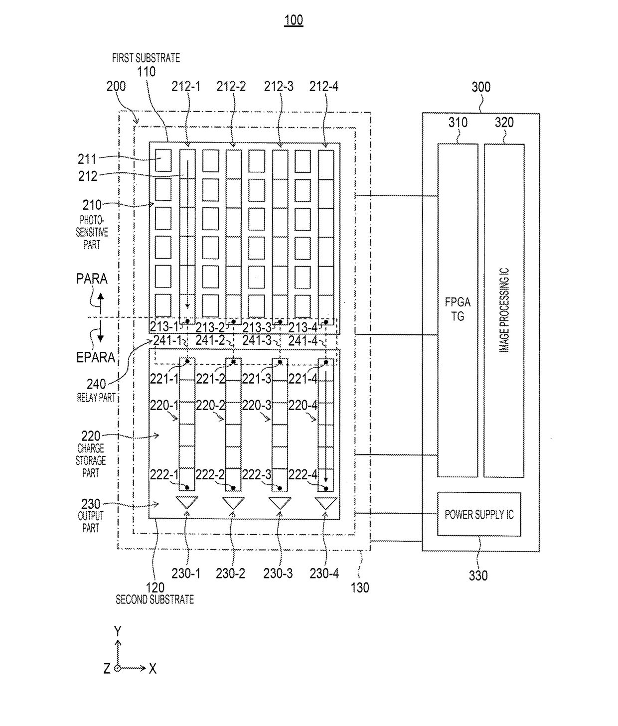
[0068]FIG. 5 is a view showing an example of the configuration of a solid-state imaging device according to a first embodiment of the present invention spread out flat. FIG. 6 is a view schematically showing a first example of a stacked substrate structure of the solid-state imaging device according to the present embodiment. FIG. 7 is a view schematically showing a second example of the stacked substrate structure of the solid-state imaging device according to the present embodiment. FIG. 8 is a view for explaining the relationship of arrangement between the photosensitive part on the first substrate and a peripheral circuit part on the second substrate which are stacked in the solid-state imaging device according to the first embodiment.

[0069]To the present solid-state imaging device 100, an image sensor similar to for example an FIT (frame interline transfer) type CCD image sensor or FT (frame transfer) type CCD image sensor can be applied. In the following description, an explan...

second embodiment

[0109]FIG. 16 is a view for explaining an example of the configuration of a solid-state imaging device according to a second embodiment of the present invention.

[0110]The difference of a solid-state imaging device 100A according to the second embodiment from the solid-state imaging device 100 in the first embodiment explained above is as follows. The solid-state imaging device 100A in the second embodiment includes a relay selecting part 250 which selectively connects a plurality of vertical transfer parts 212-1 to 212-4 and the plurality of charge storage parts 220-1 to 220-4.

[0111]In the second embodiment, a plurality of selection electrodes 251-1, 251-2, 251-3, and 251-4 are arranged in the relay part 240A on the first substrate 110A, and a plurality of selection electrodes 252-1, 252-2, 252-3, and 252-4 are arranged in the relay part 240A on the second substrate 120A. Further, on the first substrate 110A and second substrate 120A, one common through-via (TSV) 241A is formed for ...

third embodiment

[0141]FIG. 21 is a view for explaining an example of the configuration of a solid-state imaging device according to a third embodiment of the present invention.

[0142]The difference of a solid-state imaging device 100B according to the third embodiment from the solid-state imaging device 100 in the first embodiment explained above is as follows. The solid-state imaging device 100B according to the third embodiment is configured by including, on the second substrate 120B side, an output selecting part 260 which selectively connects the plurality of charge storage parts 220-1 to 220-4 and 220-5 to 220-8 and the output parts 230B-1 and 230B-2.

[0143]In the solid-state imaging device 100B in the third embodiment, in the photosensitive part 210B formed on the first substrate 110B, pixel portions 211 and vertical transfer parts 212 are arranged in a matrix comprised of six rows and eight columns. So as to correspond to this, on the second substrate 120B, eight columns of charge storage part...


PUM


Abstract

This solid-state imaging device 100 has: a photosensitive part that includes pixel portions 211, which are disposed in a matrix, and charge transfer parts 212 for transferring, by the column, the signal charge of the pixel portions; a plurality of charge storage parts 220 that accumulate the signal charges transferred by the plurality of charge transfer parts of the photosensitive part; a relay part 240 that relays the transfer of the signal charges transferred by the plurality of charge transfer parts to each charge storage part; an output part 230 that outputs the signal charges of the plurality of charge storage parts as electric signals; a first substrate 110 at which the photosensitive unit 210 is formed; and a second substrate 120 at which the charge storage part 220 and output unit 230 are formed. The first substrate and second substrate are stacked together, and the relay part 240 electrically couples the charge transfer parts of the first substrate to the charge storage parts of the second substrate by means of a connecting parts passing through the substrates outside the photosensitive region of the photosensitive part.

Description

TECHNICAL FIELD[0001]The present invention relates to a solid-state imaging device using a photoelectric conversion element which detects light and generates a charge, a method for producing a solid-state imaging device, and an electronic apparatus.BACKGROUND ART[0002]As a solid-state imaging device (image sensor) using a photoelectric conversion element which detects light and generates a charge, a CCD (charge coupled device) image sensor and CMOS (complementary metal oxide semiconductor) image sensor have been put to practical use. CCD image sensors and CMOS image sensors are widely applied as portions of digital cameras, video cameras, monitoring cameras, medical endoscopes, personal computers (PC), mobile phones and other portable terminal devices (mobile devices), and other various types of electronic apparatuses.[0003]A CCD image sensor and CMOS image sensor use photodiodes for the photoelectric conversion elements, but differ in methods of transferring photoelectrically conve...

Claims


Application Information

Patent Timeline
Patent Type & Authority Applications(United States)
IPC IPC(8): H01L27/148H04N5/378H04N5/372H01L27/146H01L23/48
CPCH01L27/14812H01L27/14634H01L27/14837H01L27/1485H04N5/378H01L27/14887H01L23/481H01L27/1469H04N5/372H01L27/14818H04N25/70H04N25/79H04N25/71H04N25/75
Inventor TAKAYANAGI, ISAOTANAKA, SHUNSUKEMORI, KAZUYAARIYOSHI, KATSUHIKOMATSUO, SHINICHIRO
Owner BRILLNICS JAPAN
Why Eureka
Try Eureka