Supercharge Your Innovation With Domain-Expert AI Agents!

Lateral passive device having dual annular electrodes

a passive device and annular electrode technology, applied in the direction of diodes, semiconductor devices, electrical apparatus, etc., can solve the problems of larger layout area of devices and larger parasitic capacitance associated with them, and achieve the effect of greatly reducing parasitic capacitance to a bottom plate (substrat)

Inactive Publication Date: 2010-10-26
INT BUSINESS MASCH CORP
View PDF17 Cites 0 Cited by
  • Summary
  • Abstract
  • Description
  • Claims
  • Application Information

AI Technical Summary

Problems solved by technology

Unfortunately, to reduce resistance for this kind of structure, the device size has to be increased, which results in a device with larger layout area and a larger associated parasitic capacitance.

Method used


Image

  • Lateral passive device having dual annular electrodes
  • Lateral passive device having dual annular electrodes
  • Lateral passive device having dual annular electrodes

Examples


Embodiment Construction

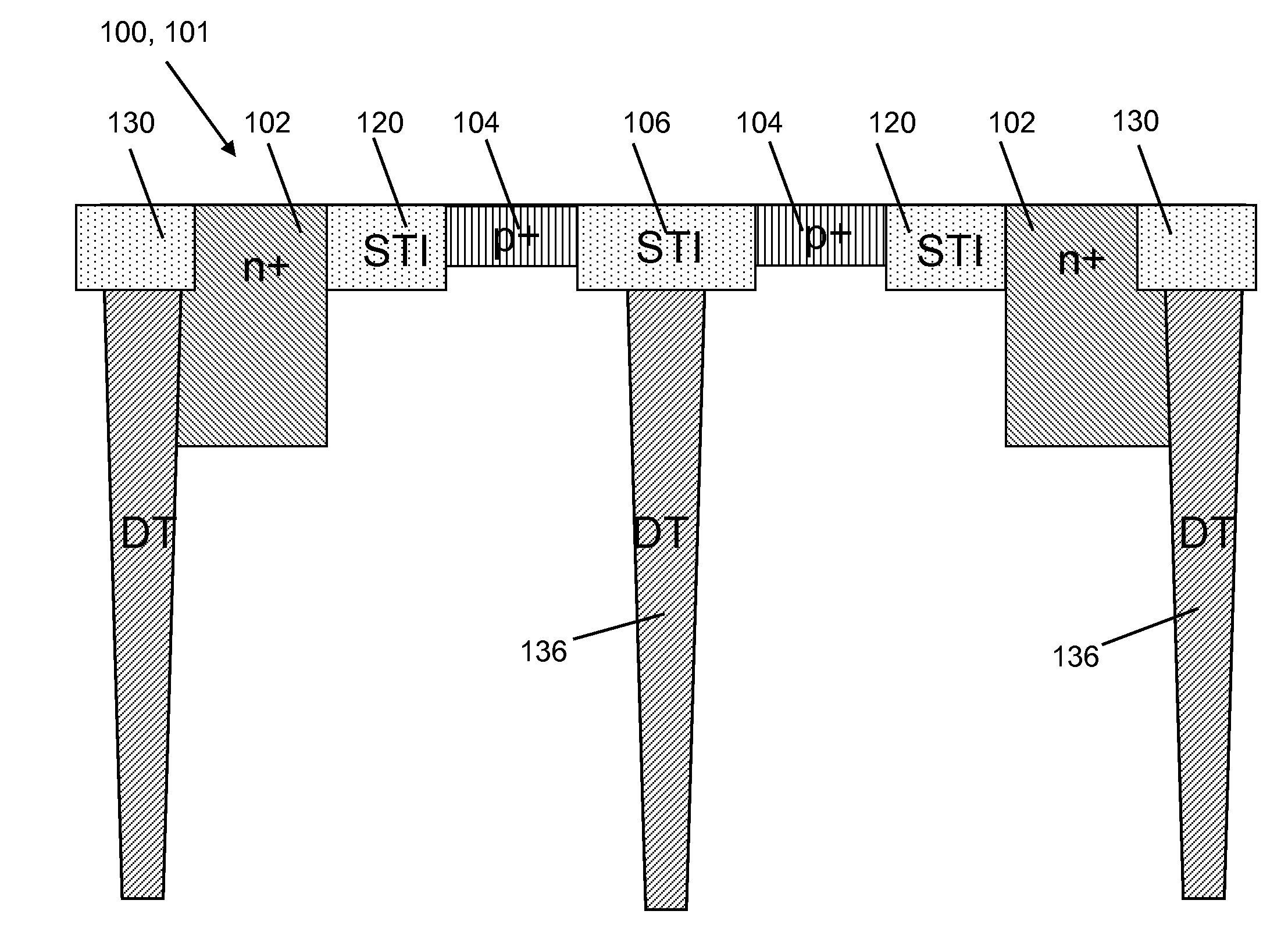
[0020]Referring to FIGS. 2-3, one embodiment of a device 100 according to the invention is shown. In one embodiment, device 100 takes the form of a lateral passive device 101 such as a lateral PN diode, a lateral PIN diode, a Schottky barrier diode or a varactor. Lateral passive device 101 includes a first annular electrode 102 surrounding a second annular electrode 104. Second annular electrode 104 surrounds a first insulator region 106, which is not annular (i.e., a non-annular, block). As used herein, the terms “first,”“second,”“third,” etc., are used for differentiation purposes only and not to denote any chronological formation or relative positioning, or to express any other meaning. Each annular electrode 102, 104 may be formed by doping a silicon substrate 110. In one embodiment, silicon substrate 110 may include a bulk silicon substrate 112 and an epitaxially grown N-silicon layer 114 thereon. It is understood, however, that the teachings of the invention may be applied to ...


PUM


Abstract

A lateral passive device is disclosed including a dual annular electrode. The annular electrodes form an anode and a cathode. The annular electrodes allow anode and cathode series resistances to be optimized to the lowest values at a fixed device area. In addition, the parasitic capacitance to a bottom plate (substrate) is greatly reduced. In one embodiment, a device includes a first annular electrode surrounding a second annular electrode formed on a substrate, and the second annular electrode surrounds an insulator region. A related method is also disclosed.

Description

GOVERNMENT INTEREST[0001]The U.S. Government has a paid-up license in this invention and the right in limited circumstances to require the patent owner to license others on reasonable terms as provided by the terms of government contract N66001-02-C-8014, awarded by the Defense Advanced Research Project Agency (DARPA).BACKGROUND OF THE INVENTION[0002]1. Technical Field[0003]The invention relates generally to semiconductor device fabrication, and more particularly, to a lateral passive device having dual annular electrodes and a related method.[0004]2. Background Art[0005]To optimize passive devices for radio frequency (RF) applications, the series resistance and parasitic capacitance need to be reduced. Referring to FIG. 1, one approach to reduce the capacitance is to increase a distance (Ld) between an anode 10 and a cathode 12, and minimize device area. Under this approach, conventional lateral devices, such as a PIN diode, PN diode, Schottky barrier diode (SBD), etc. are designed...

Claims


Application Information

Patent Timeline
Patent Type & Authority Patents(United States)
IPC IPC(8): H01L29/00
CPCH01L27/0814H01L29/417H01L29/8611H01L29/868H01L29/872H01L29/93
Inventor COLLINS, DAVID S.JOHNSON, JEFFREY B.LIU, XUEFENGORNER, BRADLEY A.RASSEL, ROBERT M.SHERIDAN, DAVID C.
Owner INT BUSINESS MASCH CORP
Features
  • R&D
  • Intellectual Property
  • Life Sciences
  • Materials
  • Tech Scout
  • Unparalleled Data Quality
  • Higher Quality Content
  • 60% Fewer Hallucinations
Learn More