Shift register, scan driving circuit and display apparatus having the same

a technology of shift register and scan driving circuit, which is applied in the direction of digital storage, static storage, instruments, etc., can solve problems such as deterioration of scan driving circui

Active Publication Date: 2009-02-03
SAMSUNG DISPLAY CO LTD
View PDF4 Cites 164 Cited by
  • Summary
  • Abstract
  • Description
  • Claims
  • Application Information

AI Technical Summary

Benefits of technology

[0020]The present invention provides a shift register capable of decreasing a parasite capacitance formed between a gate electrode and a drain electrode of a pull-up transistor to prevent a floating of the pull-up transistor outputting a scan signal.
[0031]Therefore, a parasite capacitance between a gate electrode of a pull-up transistor that outputs the scan signal and a drain electrode of the pull-up transistor is decreased so that a floating of the gate electrode of the pull-up transistor is prevented. In addition, a floating of a source electrode of the pull-up transistor or the output terminal is also prevented.

Problems solved by technology

Therefore, when the scan driving circuit includes the amorphous silicon TFT, the parasite capacitance may be formed between the gate and drain electrodes of the second transistor, and the first node floats, thereby deteriorating the scan driving circuit.

Method used


Image

  • Shift register, scan driving circuit and display apparatus having the same
  • Shift register, scan driving circuit and display apparatus having the same
  • Shift register, scan driving circuit and display apparatus having the same

Examples


Embodiment Construction

[0042]It should be understood that the exemplary embodiments of the present invention described below may be varied modified in many different ways without departing from the inventive principles disclosed herein, and the scope of the present invention is therefore not limited to these particular following embodiments. Rather, these embodiments are provided so that this disclosure will be via and complete, and will fully convey the concept of the invention to those skilled in the art by way of example and not of limitation.

[0043]Hereinafter, the present invention will be described in detail with reference to the accompanying drawings.

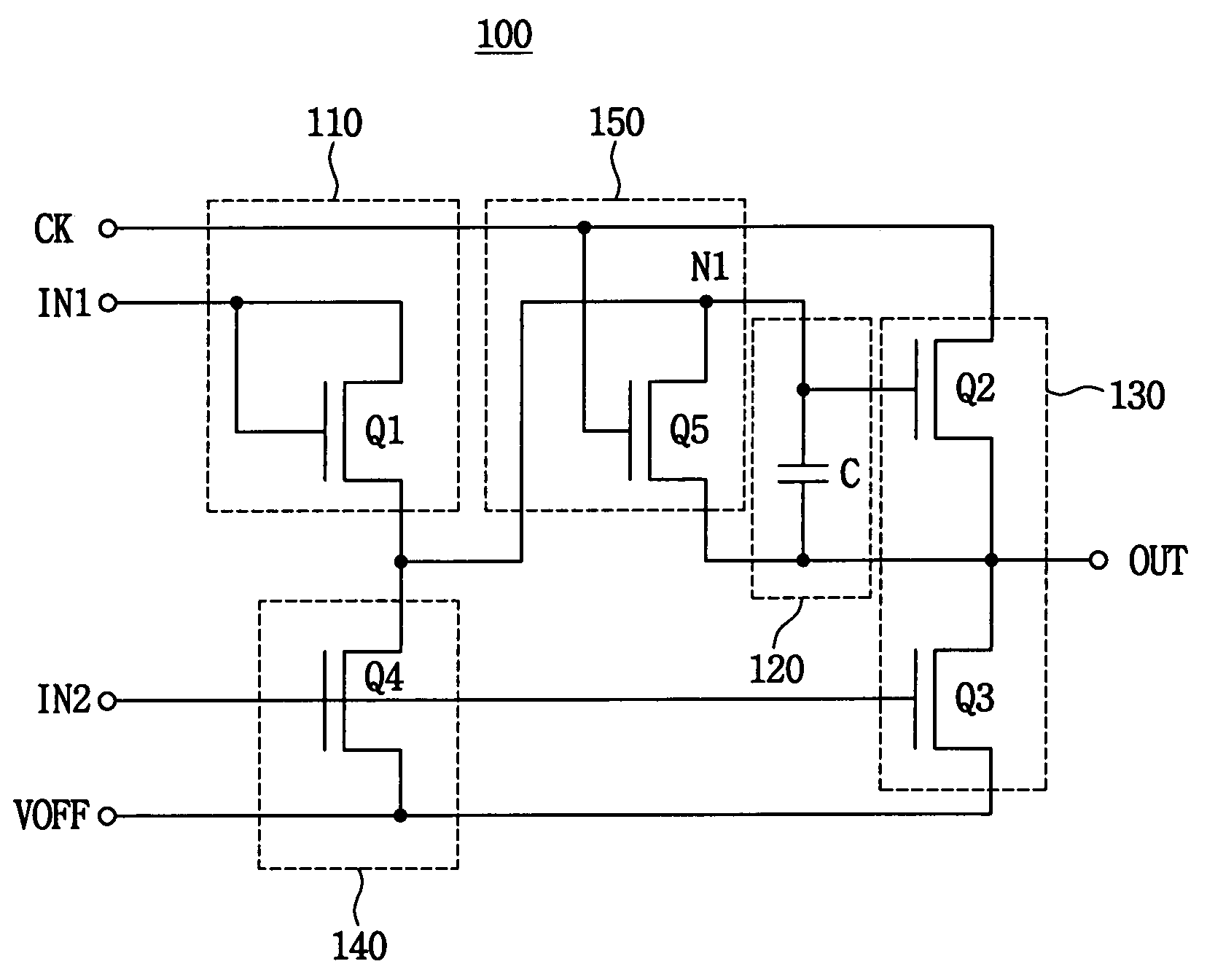
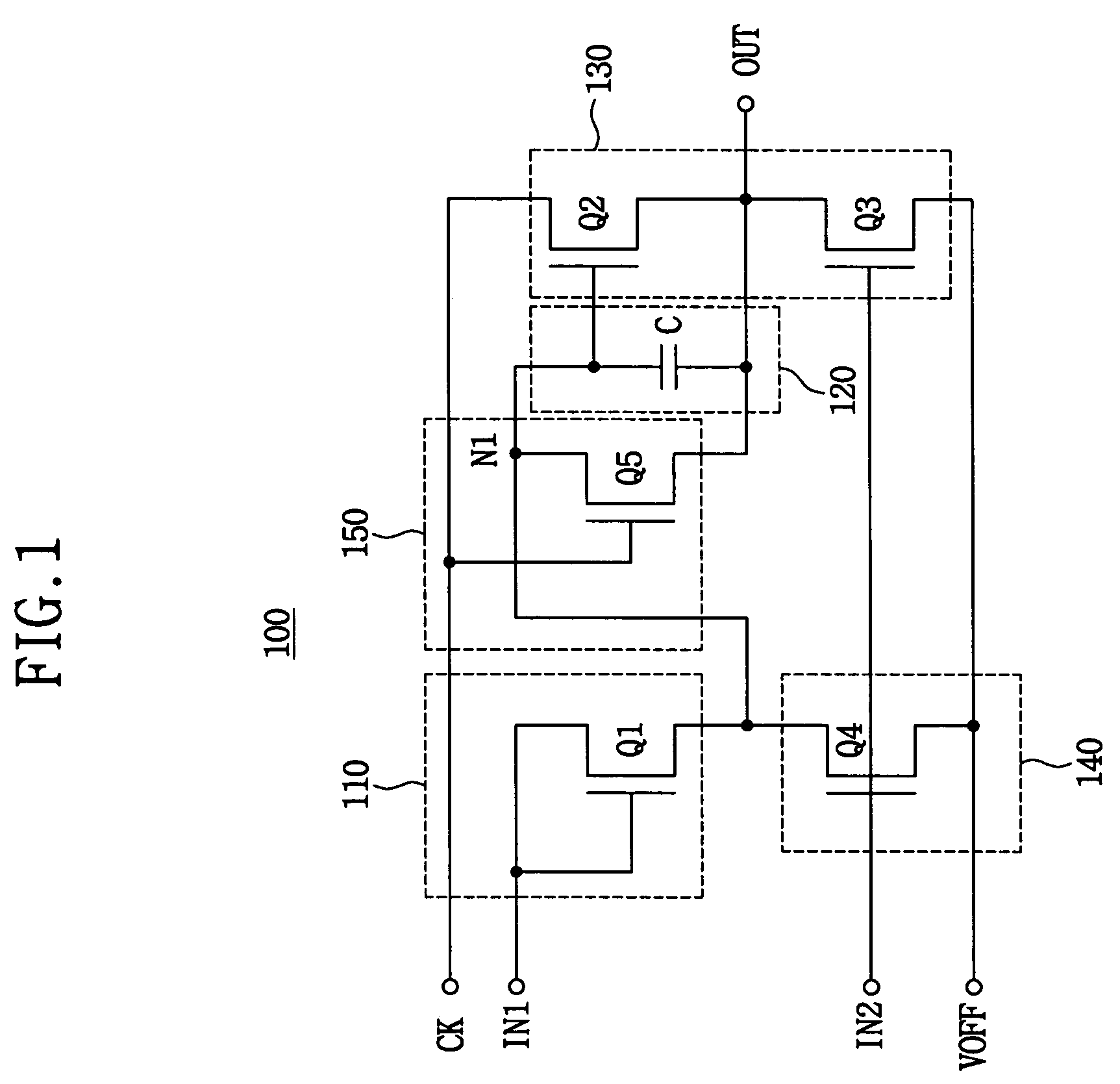
[0044]FIG. 1 is a circuit diagram showing a unit stage of a shift register in accordance with an exemplary embodiment of the present invention. A scan driving circuit having the unit stage includes transistors having amorphous silicon thin film transistors (a-Si TFTs). The unit stage prevents a floating of a gate electrode of a second transistor (Q2).

[0...


PUM

PropertyMeasurementUnit
voltageaaaaaaaaaa
lengthaaaaaaaaaa
lengthaaaaaaaaaa

Abstract

A shift register includes a plurality of stages to generate a plurality of output signals, in sequence. Each of the stages includes a driving circuit, a charging circuit, a discharging circuit and a holding circuit. The driving circuit is configured to generate a first output signal in response to a first clock signal or a second clock signal having a phase different from the first clock signal. The charging circuit is configured to charge an electric charge in response to a scan start signal or a second output signal of an adjacent previous stage. The discharging circuit is configured to discharge the electric charge in response to a third output signal of an adjacent next stage. The holding circuit is configured to maintain the first output signal within a first voltage when the first output signal is in an inactive state. Therefore, a parasite capacitance is decreased to prevent a floating of a pull-up transistor.

Description

CROSS-REFERENCE OF RELATED APPLICATIONS[0001]The present application claims priorities from Korean Patent Application No. 2003-46503, filed on Jul. 9, 2003 and Korean Patent Application No. 2003-72889, filed on Oct. 20, 2003, the disclosure of which is hereby incorporated herein by reference in their entireties.BACKGROUND OF THE INVENTION[0002]1. Field of the Invention[0003]The present invention relates to a shift register, a scan driving circuit having the shift register and a display apparatus having the shift register.[0004]2. Description of the Related Art[0005]A data driver integrated circuit or a gate driver integrated circuit may be integrated into a liquid crystal display (LCD) panel so as to decrease a manufacturing cost and a size of an LCD apparatus. In order to integrate the driver integrated circuits, a scan driving circuit of the LCD panel has a simplified structure.[0006]The scan driving circuit includes a shift register to generate a gate pulse, and applies the gate ...

Claims


Application Information

Patent Timeline
Patent Type & Authority Patents(United States)
IPC IPC(8): G09G3/36G02F1/133G09G3/20G11C19/00G11C19/18G11C19/28
CPCG09G3/3677G11C19/00G11C19/184G11C19/28G09G2310/0286
Inventor MOON, SEUNG-HWAN
Owner SAMSUNG DISPLAY CO LTD
Why Eureka
Try Eureka