Testing apparatus and method for thin film transistor display array

Inactive Publication Date: 2005-02-03
PRIMETECH INT CORP
View PDF2 Cites 159 Cited by
  • Summary
  • Abstract
  • Description
  • Claims
  • Application Information

AI Technical Summary

Benefits of technology

[0009] It is therefore an object of the invention to provide a testing method for thin film transistor display array, for testing the small value of a pixel capacitor in parallel to the large parasitic capacitance o

Problems solved by technology

The measuring signal is too small in yield testing of quality control step, so that the accuracy is not good enough.
However, the parasitic capacitance is also charged simultaneously, and the signal is difficult to se

Method used


Image

  • Testing apparatus and method for thin film transistor display array
  • Testing apparatus and method for thin film transistor display array
  • Testing apparatus and method for thin film transistor display array

Examples


Embodiment Construction

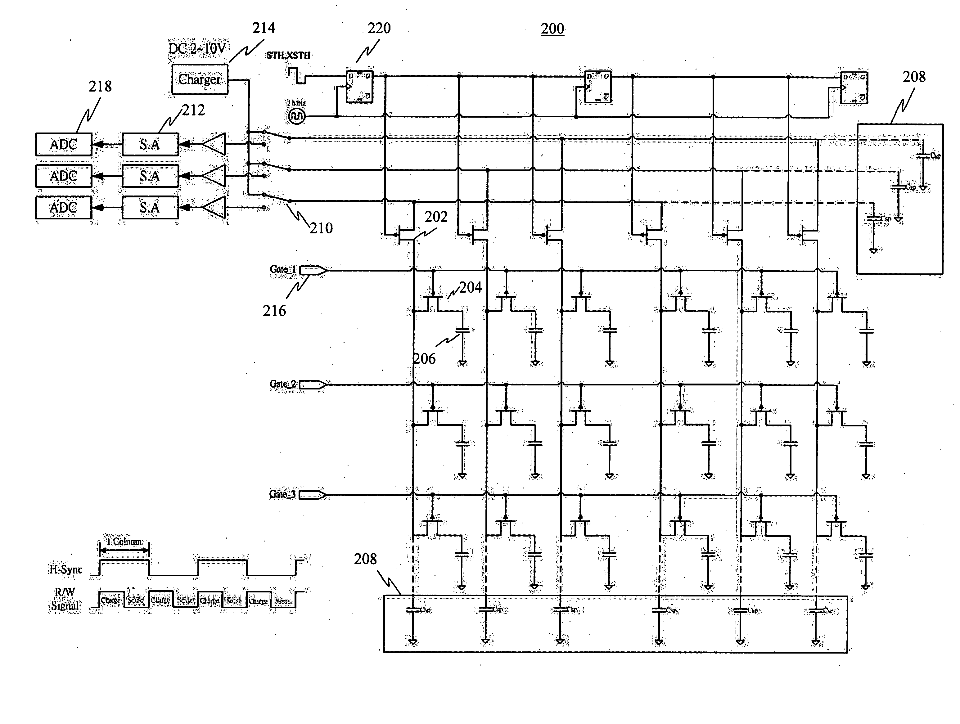
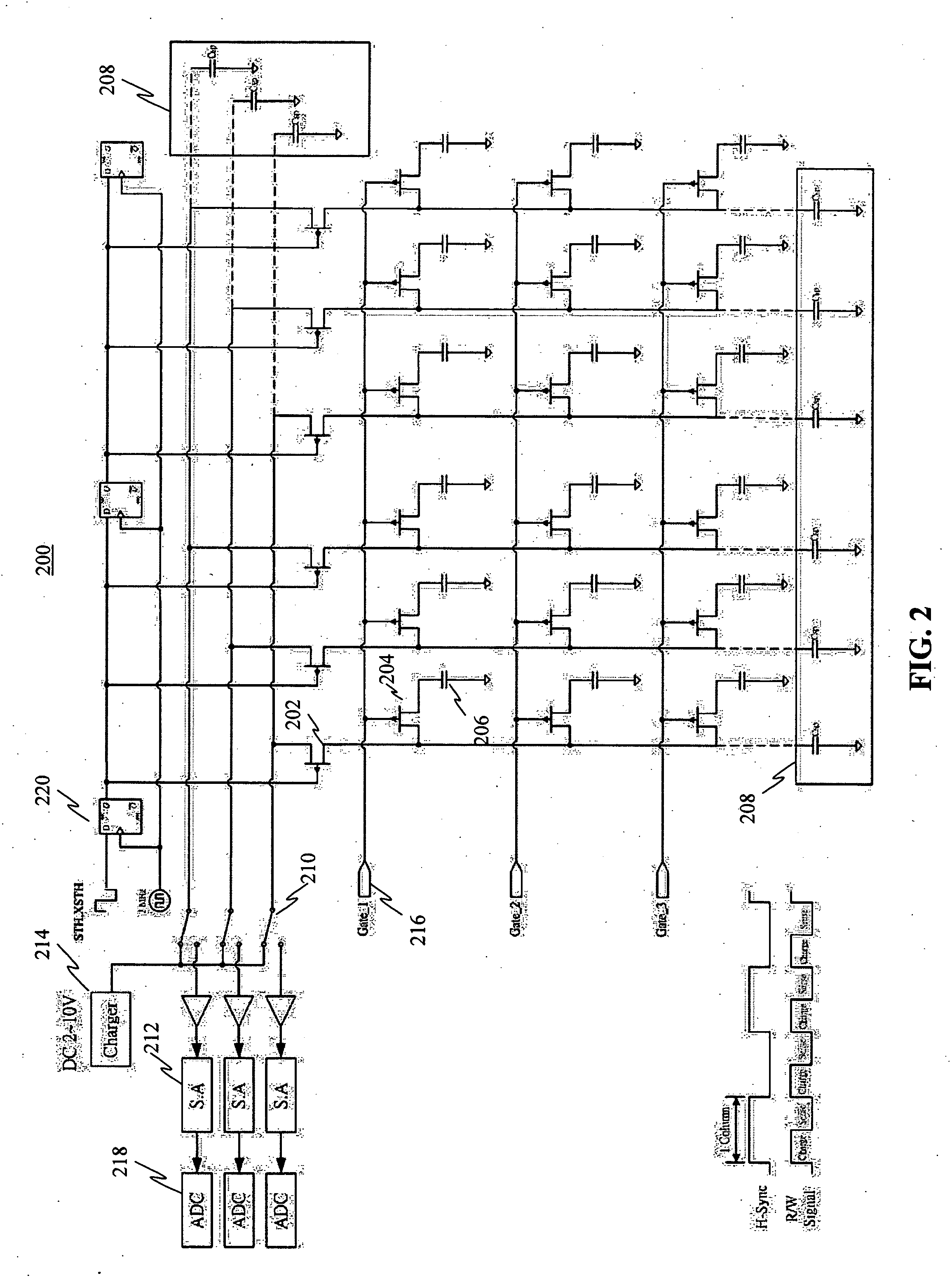
[0022] Referring to FIG. 2, FIG. 2 is a connection block diagram of a testing circuit for low temperature poly-Si thin film transistor array 200 in according to one embodiment of the present invention. The gate of the column switching-transistor 202 (or the read / write switching transistor) is controlled to switch ON or switch OFF by the gate control circuit 220 of the column switching-transistor 202, to connect the column, for example column n (n=1 to N, N is the total column) from the source / drain to the DC charging source or the testing circuit, the gate of the pixel switching transistor 204 is connected to the row switching-transistor 216 of row k (k=1 to K, K is the total row), the source of the pixel switching transistor 204 is connected to the drain of the column switching-transistor 202, and the drain of the pixel switching transistor 204 is connected to the positive electrode of the pixel capacitor, the negative electrode of the pixel capacitor is connected to the common of ...


PUM


Abstract

The present invention discloses a testing circuit and method for thin film transistor display array, for testing the yield of thin film transistor array. The testing circuit comprising: An array tester, a test panel (DUT), a sense amplifier array. The sense amplifier is composed by a plurality of trans- impedance amplifier unit and a plurality of parasitic capacitance discharge circuit unit. Every sense amplifier includes: a trans-impedance amplifier, which is implemented by an operational amplifier, two switches and an operation capacitance, the trans-impedance amplifier is used to form an integrated circuit, the output is transmitted to a sampling/hold circuit via a switch; a parasitic capacitance discharge circuit is used to form a discharge rout for the charge of the parasitic capacitance.

Description

BACKGROUND OF THE INVENTION [0001] 1. Field of the Invention [0002] The present invention relates to a circuit testing method. In particular, the present invention relates to a testing method for pixel storage capacitance of a thin film transistor display circuit. A reliable and precise testing result of the yield can be obtained in conditions that parasitic capacitance is much larger than a pixel capacitance. [0003] 2. Description of the Related Art [0004] The pixels of liquid crystal display (LCD) or organic liquid crystal display (OLED) become more and more, the area of large area display also become larger and larger, the parasitic capacitance Csp of the source line of the thin film transistor would be much more larger than the pixel storage capacitance Cs. The measuring signal is too small in yield testing of quality control step, so that the accuracy is not good enough. [0005] Generally, to measure the yield of the pixel capacitance, it is always to charge the pixel capacitanc...

Claims


Application Information

Patent Timeline
IPC IPC(8): G01R31/319G09G3/00
CPCG09G3/006G01R31/31924
Inventor KUO, KUANG I.TIEN, HSIAO TUNG
Owner PRIMETECH INT CORP
Why Eureka
Try Eureka