Integrated circuits including finfet devices with lower contact resistance and reduced parasitic capacitance and methods for fabricating the same

a technology of integrated circuits and finfets, which is applied in the direction of semiconductor devices, electrical devices, transistors, etc., can solve the problems of higher parasitic capacitance, contact formation to non-planar source and drain regions of fins,

Active Publication Date: 2014-08-07
IBM CORP +1
View PDF15 Cites 155 Cited by
  • Summary
  • Abstract
  • Description
  • Claims
  • Application Information

AI Technical Summary

Problems solved by technology

One important challenge with the implementation of FINFETs is the formation of contacts to the non-planar source and drain regions of the fins.
However, during contact formation, conductive contact-forming material can be deposited between the lower sections of unmerged fins, leading to higher parasitic capacitance.

Method used


Image

  • Integrated circuits including finfet devices with lower contact resistance and reduced parasitic capacitance and methods for fabricating the same
  • Integrated circuits including finfet devices with lower contact resistance and reduced parasitic capacitance and methods for fabricating the same
  • Integrated circuits including finfet devices with lower contact resistance and reduced parasitic capacitance and methods for fabricating the same

Examples


Embodiment Construction

[0013]The following Detailed Description is merely exemplary in nature and is not intended to limit the various embodiments or the application and uses thereof Furthermore, there is no intention to be bound by any theory presented in the preceding background or the following detailed description.

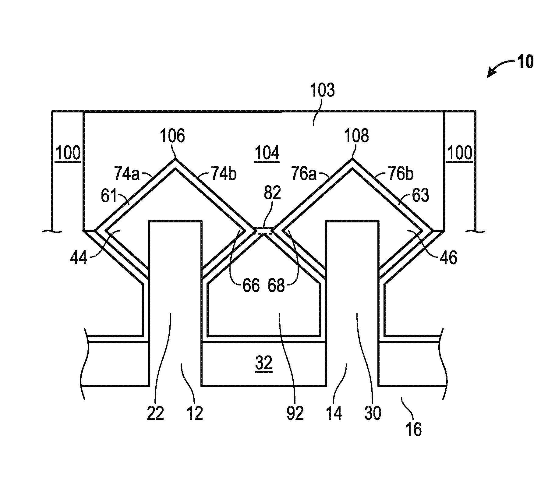
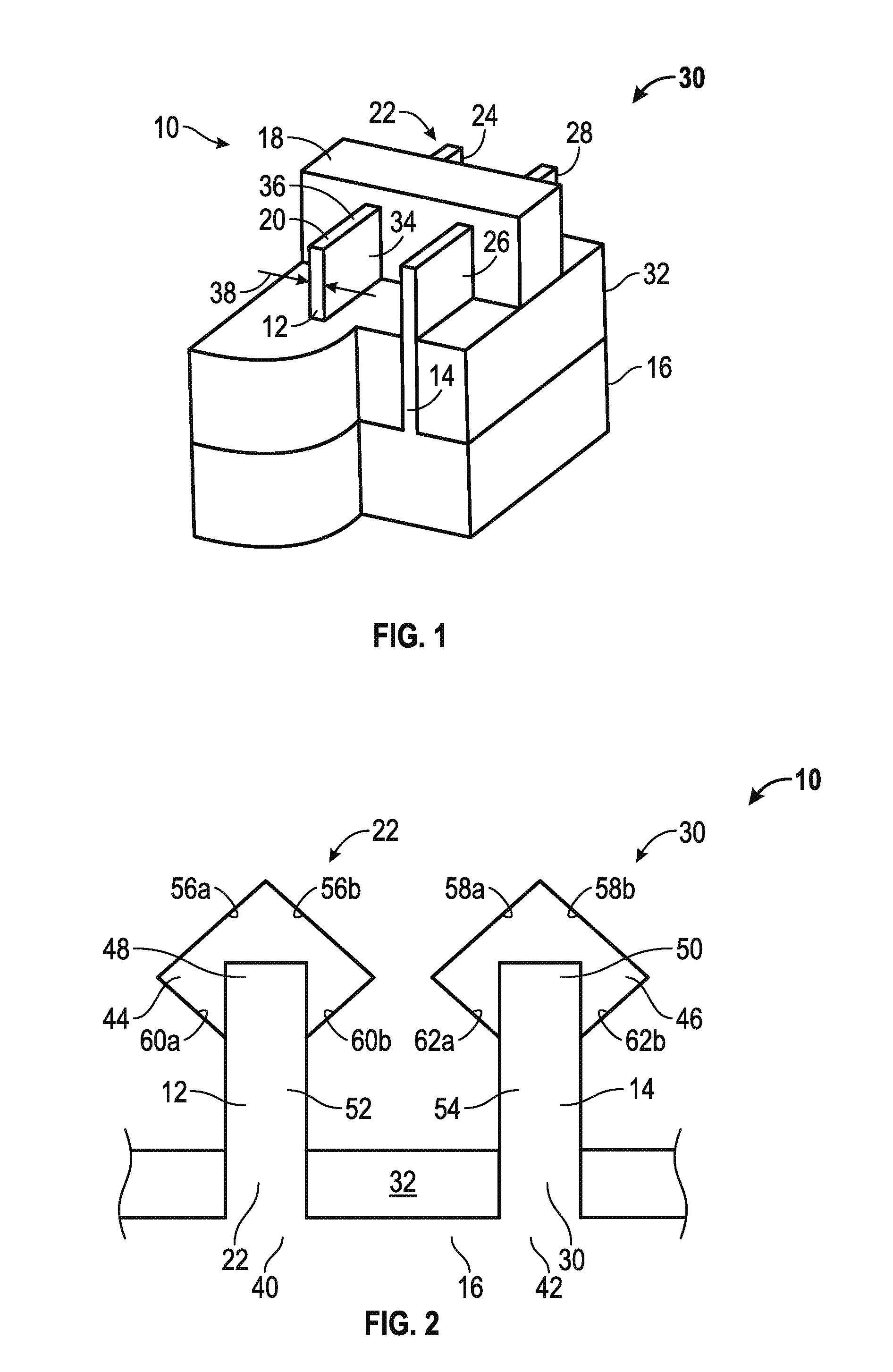
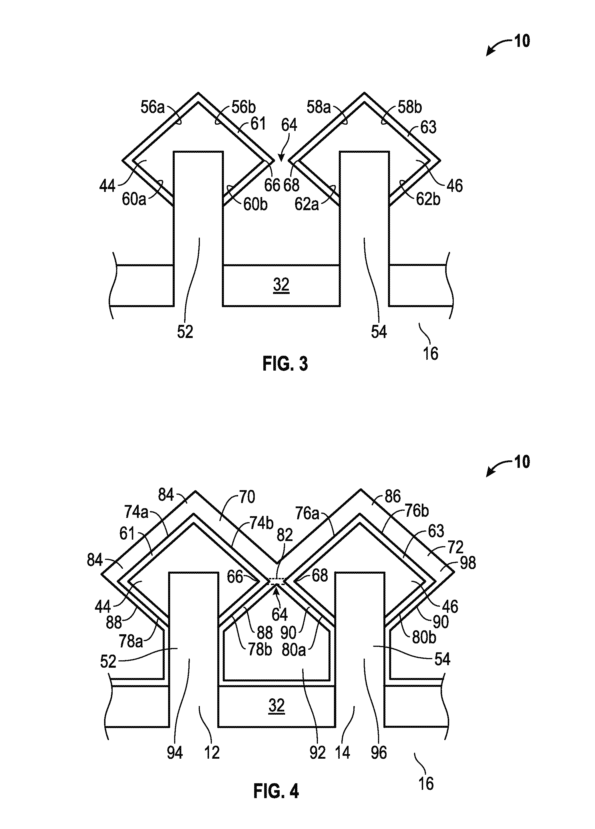
[0014]Integrated circuits (ICs) can be designed with millions of transistors. Many ICs are designed using metal oxide semiconductor (MOS) transistors, also known as field effect transistors (FETs) or MOSFETs. Although the term “MOS transistor” properly refers to a device having a metal gate electrode and an oxide gate insulator, that term used herein refers to any device that includes a conductive gate electrode (whether metal or other conductive material) that is positioned over a gate insulator (whether oxide or other insulator) which, in turn, is positioned over a semiconductor substrate. One type of MOS transistor used in the design of ICs is a FINFET, which can be fabricated as a P-chan...


PUM

PropertyMeasurementUnit
thicknessaaaaaaaaaa
thicknessaaaaaaaaaa
thicknessaaaaaaaaaa

Abstract

Integrated circuits and methods for fabricating integrated circuits are provided. In one example, an integrated circuit includes a semiconductor substrate. A first fin and a second fin are adjacent to each other extending from the semiconductor substrate. The first fin has a first upper section and the second fin has a second upper section. A first epi-portion overlies the first upper section and a second epi-portion overlies the second upper section. A first silicide layer overlies the first epi-portion and a second silicide layer overlies the second epi-portion. The first and second silicide layers are spaced apart from each other to define a lateral gap. A dielectric spacer is formed of a dielectric material and spans the lateral gap. A contact-forming material overlies the dielectric spacer and portions of the first and second silicide layers that are laterally above the dielectric spacer.

Description

TECHNICAL FIELD[0001]The technical field relates generally to integrated circuits and methods for fabricating integrated circuits, and more particularly relates to integrated circuits including FINFET devices with lower contact resistance and reduced parasitic capacitance and methods for fabricating such integrated circuits.BACKGROUND[0002]Transistors such as metal oxide semiconductor field effect transistors (MOSFETs) or simply field effect transistors (FETs) or MOS transistors are the core building blocks of the vast majority of semiconductor integrated circuits (ICs). A FET includes source and drain regions between which a current can flow through a channel under the influence of a bias applied to a gate electrode that overlies the channel. Some semiconductor ICs, such as high performance microprocessors, can include millions of FETs. For such ICs, decreasing transistor size and thus increasing transistor density has traditionally been a high priority in the semiconductor manufac...

Claims


Application Information

Patent Timeline
Patent Type & Authority Applications(United States)
IPC IPC(8): H01L27/088H01L21/28
CPCH01L21/28H01L27/0886H01L21/823431H01L29/66795H01L29/785H01L29/0653H01L29/41791H01L29/458H01L29/7853
Inventor CAI, XIUYUXIE, RUILONGKHAKIFIROOZ, ALICHENG, KANGGUO
Owner IBM CORP
Why Eureka
Try Eureka