Fabrication of self-aligned via holes in polymer thin films

a thin film, self-aligned technology, applied in the direction of semiconductor/solid-state device manufacturing, basic electric elements, electric apparatus, etc., can solve the problems of only partially cured or not cured post material, and achieve the effect of low cost and efficien

Inactive Publication Date: 2010-12-28
GULA CONSULTING LLC
View PDF23 Cites 6 Cited by
  • Summary
  • Abstract
  • Description
  • Claims
  • Application Information

AI Technical Summary

Benefits of technology

[0011]According to the present invention, a low-cost and efficient method of fabrication is disclosed that can produce self-aligned vias in dielectric polymer films that provides electrical connection between a top conductor and a bottom conductor.

Problems solved by technology

In this case, the post material is not cured or only partially cured before the dielectric deposition.

Method used


Image

  • Fabrication of self-aligned via holes in polymer thin films
  • Fabrication of self-aligned via holes in polymer thin films
  • Fabrication of self-aligned via holes in polymer thin films

Examples


Embodiment Construction

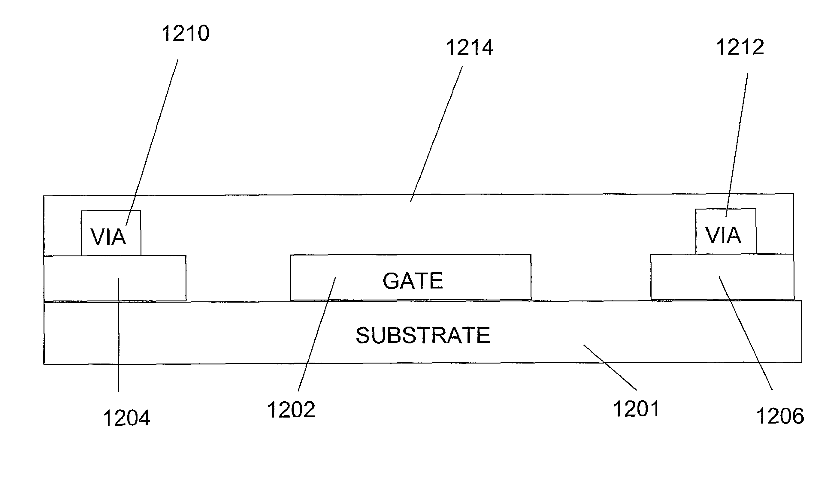
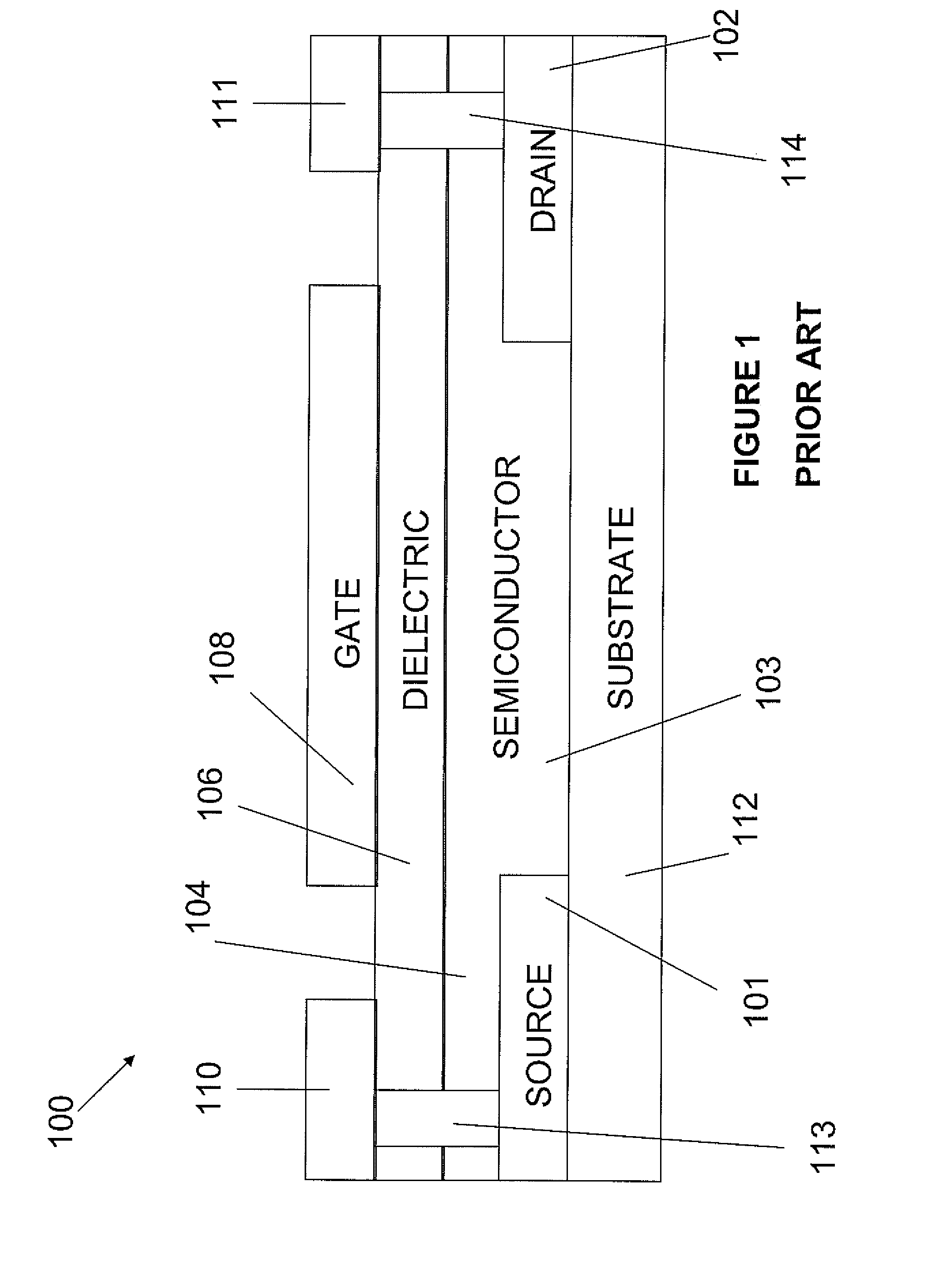
[0039]The via formation according to the present invention is described with respect to the fabrication of a top gate organic transistor in FIGS. 2-4 and 9-11 and with respect to the fabrication of a bottom gate organic transistor in FIGS. 12-18.

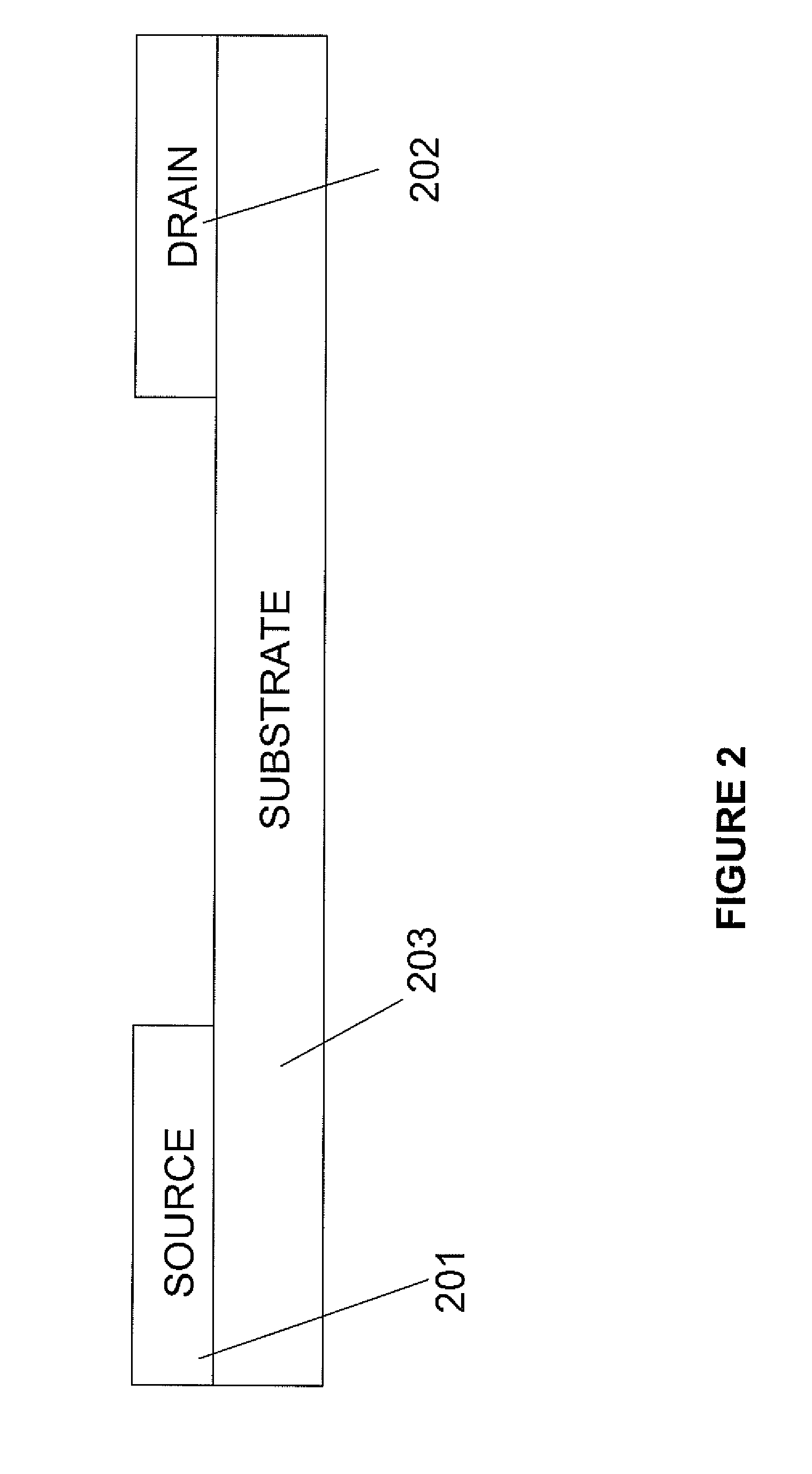
[0040]Referring now to FIG. 2, a source and drain conductor, 201 and 202, respectively, is patterned on insulating substrate 203. The source / drain conductor can be of any material that conducts electricity, including metals, conducting polymers, or nano-particle ink. The preferred deposition means depends on the material, including sublimation and evaporation of a solid source, or deposition by means of a liquid. Patterning can be achieved through a shadow mask, by directly depositing the pattern of interest, or by means of a deposition followed by removal of unwanted materials. The substrate must be electrically insulating, consisting of either flexible or rigid material. Flexible substrate materials include PET, PEN, Kapton, mylar, and pap...


PUM

PropertyMeasurementUnit
conductiveaaaaaaaaaa
dielectricaaaaaaaaaa
heightaaaaaaaaaa

Abstract

A low-cost and efficient process produces self-aligned vias in dielectric polymer films that provides electrical connection between a top conductor and a bottom conductor. The process is achieved by printing conductive posts on the first patterned conductive layer, followed by the deposition of an unpatterned layer dielectric, followed by the deposition of a second patterned conductive layer. The vias are formed during the flash annealing of the post after the dielectric is deposited, but before the second conductive layer is deposited. In this process, the post material is annealed with a flash of light, resulting in a release of energy which removes the dielectric on the top of the post.

Description

FIELD OF INVENTION[0001]The present invention relates to organic transistors used in printed circuits and, more particularly to a method of fabricating via holes in polymer dielectrics to connect one conductive layer with another.DESCRIPTION OF RELATED ART[0002]Organic field-effect transistors (oFETs) have been proposed for a number of applications including displays, electronic barcodes and sensors. Low cost processes, large-area circuits and the chemically active nature of organic materials are the chief driving forces to make oFETs important in various applications. Many of these objectives depend on a method of fabrication utilizing printing techniques such as flexography, gravure, silk screen and inkjet printing.[0003]Printed top gate and bottom gate structured transistors and circuits have been demonstrated in the past. Usually, such a system consists of printed semiconductor, dielectric and gate conductors on flexible substrates.[0004]Referring now to FIG. 1, a cross-sectiona...

Claims


Application Information

Patent Timeline
Patent Type & Authority Patents(United States)
IPC IPC(8): H01L21/4763
CPCH01L51/105H01L51/0005H01L51/0026H01L51/0545H01L51/0541H10K71/135H10K71/40H10K10/464H10K10/84H10K10/466
Inventor MOHAPATRA, SIDDHARTHDIMMLER, KLAUSJENKINS, PATRICK H
Owner GULA CONSULTING LLC
Why Eureka
Try Eureka