Time to digital converting circuit and related method

a digital conversion and time-to-digital conversion technology, applied in the field of time-to-digital conversion (tdc) circuits, can solve problems such as large circuit area

Active Publication Date: 2011-01-18
REALTEK SEMICON CORP
View PDF4 Cites 11 Cited by
  • Summary
  • Abstract
  • Description
  • Claims
  • Application Information

AI Technical Summary

Problems solved by technology

The conventional TDC circuit and method thereof require the use of a complete delay circuit, however, resulting in a larger circuit area.

Method used


Image

  • Time to digital converting circuit and related method
  • Time to digital converting circuit and related method
  • Time to digital converting circuit and related method

Examples


first embodiment

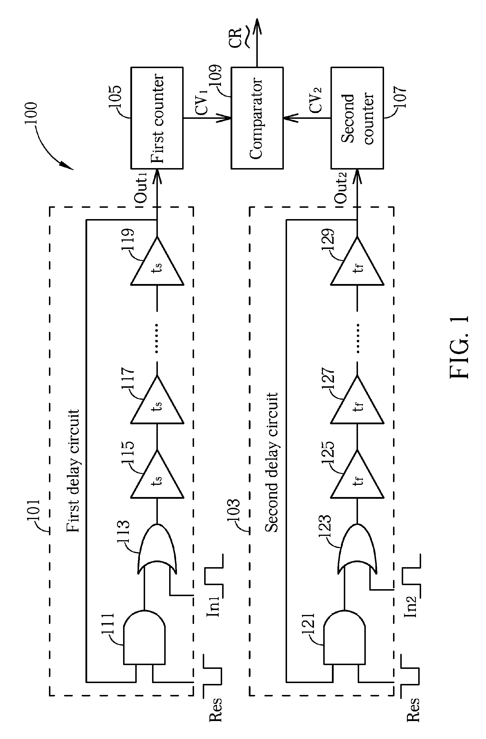
Please refer to FIG. 1. FIG. 1 is a block diagram illustrating a TDC circuit 100 according to the present invention. As shown in FIG. 1, the TDC circuit 100 includes a first delay circuit 101 (which is a periodic delay circuit), a second delay circuit 103 (which is a periodic delay circuit), a first counter 105, a second counter 107, and a comparator 109. The first delay circuit 101 includes at least one first delay stage (first delay stages 115, 117, 119 in this exemplary embodiment) for delaying a first input signal In1 to generate a first output signal Out1 accordingly. Similarly, the second delay circuit 103 includes at least one second delay stage (second delay stages 125, 127, 129 in this exemplary embodiment) for delaying a second input signal In2 to generate a second output signal Outs accordingly, where the second input signal In2 is a predetermined reference signal in this exemplary embodiment.

As shown in FIG. 1, the first counter 105 coupled to the first delay circuit 101...

second embodiment

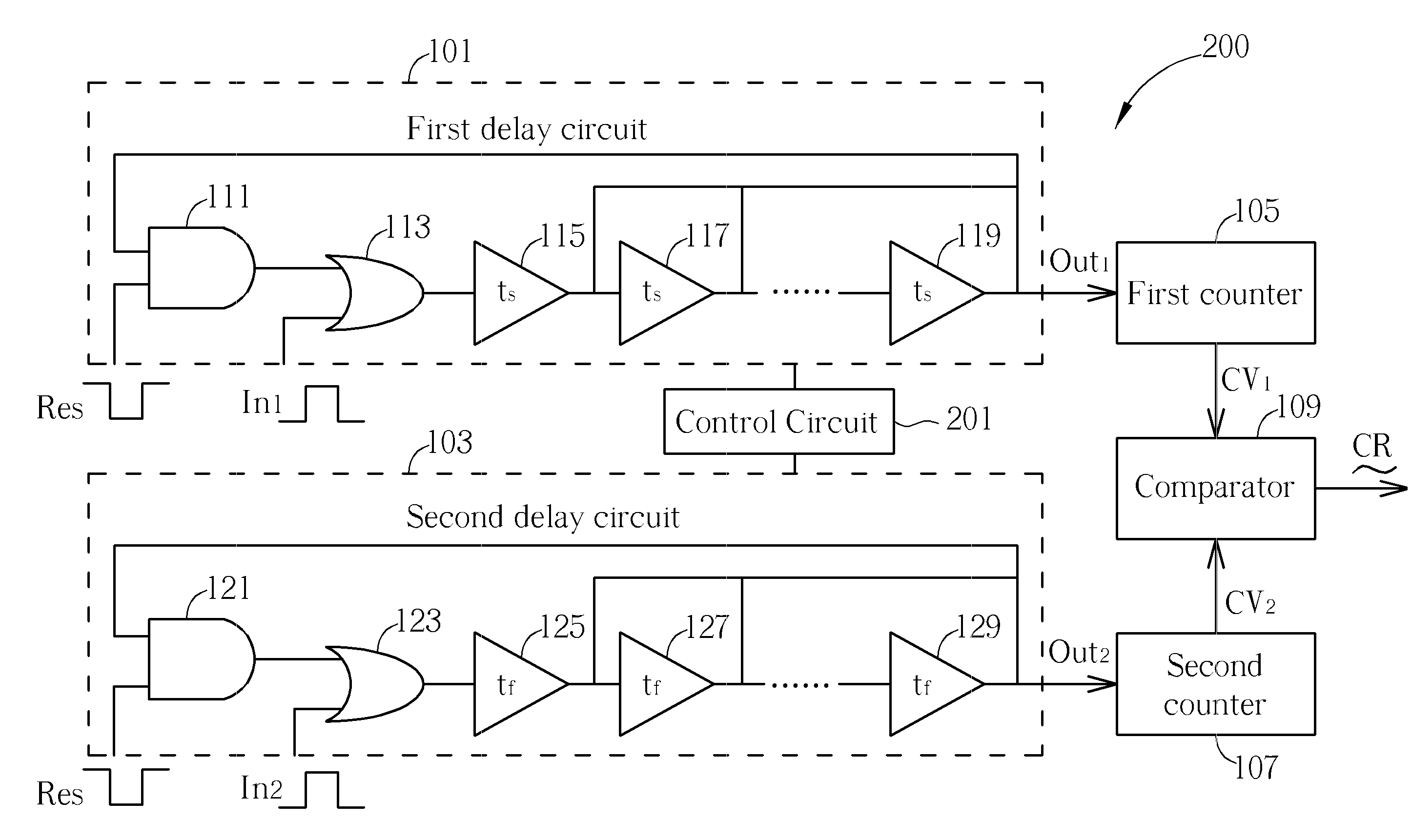
Please refer to FIG. 2; FIG. 2 is a block diagram illustrating a TDC circuit 200 according to the present invention. The circuit structure of the TDC circuit 200 shown in FIG. 2 is similar to that of the TDC circuit 100 shown in FIG. 1. The difference is that the TDC circuit 200 shown in FIG. 2 further includes a control circuit 201 to control how many delay stages are used in the first and second delay circuits 101, 103 to generate the required output signal. That is, the control circuit 201 is used to make the output signals Out1 and Out2 correspond to a portion of the delay stages in the first delay circuit and second delay circuit, respectively. In this way, the application field of the disclosed TDC circuit in the present invention is broadened. In addition, the use of the control circuit 201 is not necessary for selecting the required number of the first / second delay stages to selectively output the output signals of different delay situations. Other schemes for selectively ch...


PUM


Abstract

A TDC circuit includes: a first delay circuit, including at least one first delay stage for delaying a first input signal to generate a first output signal; a second delay circuit, including at least one second delay stage for delaying a second input signal to generate a second output signal; a first counter, for computing the first output signal to generate a first counter value; a second counter, for computing the second output signal to generate a second counter value; and a comparator, for comparing the first counter value and the second counter value to generate a comparing result signal; wherein the first delay stage has a larger delay amount than the second delay stage, the first counter starts before the second counter, and the comparator outputs the comparing result signal when the second counter value falls within a predetermined range of the first counter value.

Description

BACKGROUND OF THE INVENTION1. Field of the InventionThe present invention relates to time to digital converting (TDC) circuits, and more particularly, to a time to digital converting (TDC) circuit utilizing delay circuits to generate periodic delay signals and a related method.2. Description of the Prior ArtIn general, a time to digital converting (TDC) circuit is utilized for measuring the delay level of a signal under test and transferring the abstract delay level into a physical delay amount provided by delay stage(s). That is, the time to digital converting circuit is capable of expressing the delay level of a signal under test by the number of delay stages. Taking a conventional time to digital converting circuit as an example, a first signal and a second signal are sent to a first delay circuit and a second delay circuit respectively. As a result, after a certain amount of time, the second signal will catch up with the first signal. When the two signals (i.e., the first signal...

Claims


Application Information

Patent Timeline
Patent Type & Authority Patents(United States)
IPC IPC(8): H03M1/00
CPCG04F10/005
Inventor CHEN, YI-LIN
Owner REALTEK SEMICON CORP
Why Eureka
Try Eureka