Spatial information detecting device and photodetector suitable therefor

a technology of information detection and detection device, which is applied in the field of spatial information detection device and photodetector, can solve the problems of inability to downsize the photoelectric conversion portion for receiving the light from the target space to generate electric charges, information to be detected prior to the charge transfer channel, etc., and achieves the effect of preventing saturation phenomenon, high operation reliability, and downsizing the photoelectric conversion portion

Inactive Publication Date: 2011-01-25
PANASONIC SEMICON SOLUTIONS CO LTD
View PDF16 Cites 18 Cited by
  • Summary
  • Abstract
  • Description
  • Claims
  • Application Information

AI Technical Summary

Benefits of technology

[0006]In consideration of the above problem, a primary concern of the present invention is to provide a spatial information detecting device with high operation reliability, which is capable of downsizing a photoelectric converting portion, and preventing saturation phenomenon even when a large amount of undesired electric charges is generated by receiving the light from the target space.

Problems solved by technology

In this configuration, however, since the removal of the undesired electric charges is performed in the charge transfer channel, the so-called saturation phenomenon happens when the undesired electric charges generated by receiving the light from the target space exceed a photoelectric conversion capacity.
In this case, there is a possibility that the information to be detected is lost prior to the charge transfer channel.
However, there is a problem that a photoelectric converting portion for receiving the light from the target space to generate the electric charges cannot be downsized.

Method used


Image

  • Spatial information detecting device and photodetector suitable therefor
  • Spatial information detecting device and photodetector suitable therefor
  • Spatial information detecting device and photodetector suitable therefor

Examples


first embodiment

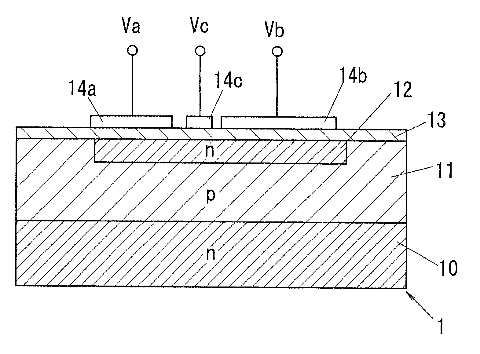
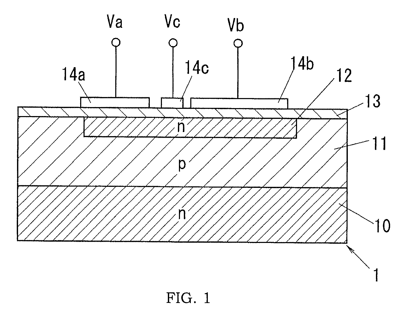
[0055]The spatial information detecting device of this embodiment comprises a light emission source configured to project a light intensity-modulated by a modulation signal as a signal light into a target space, a photodetecting portion configured to provide a received light output reflecting a fluctuation component of the signal light by separating a constant amount of a bias component from electric charges corresponding to a received light amount detected from the target space at a timing synchronized with the modulation signal, and a signal processing portion configured to detect the spatial information of the target space (e.g., a distance to an object in the target space) by use of the received light output. In the following embodiments, the photodetecting portion is provided by a photodetector. In addition, to avoid that the explanation of the present invention becomes complicated, only a minimum unit cell of the photodetector and its operation are explained in some situations...

second embodiment

[0134]The present embodiment is characterized by using the photodetector capable of automatically changing the amount of electrons separated as the undesired electric charges according to the received-light amount without using an external circuit for controlling the potential barrier B1.

[0135]That is, as a configuration for automatically adjusting the amount of the undesired electric charges, the photodetector 1 of the present embodiment has a holding well 15 formed on the general surface of a device formation layer 11 at a different position from the well 12, as shown in FIG. 9A. The holding well 15 has the same conductive type as the well 12, and a lower impurity concentration than the well 12. That is, the conductive type of the holding well 15 is n+. In addition, a holding electrode 14d is disposed at a position corresponding the holding well 15 to through an insulating layer 13, and a gate electrode 14e is disposed at a position corresponding to a region between the well 12 an...

third embodiment

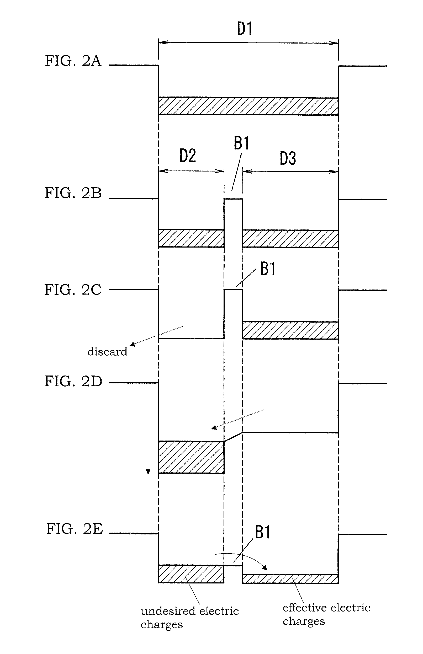
[0158]In the present embodiment, as in the second embodiment, the charge holding portion D4 is formed, and the capacity of the charge separating portion D2 is automatically determined according to the received-light amount of the environmental light. The present embodiment is characterized by modulating the intensity of light projected from the light emission source in the lighting period by a modulation signal having a constant frequency, and taking out received-light outputs corresponding to received-light amounts, which are obtained at timings synchronized with two different phase zones of the modulation signal. In addition, a since wave is used as the waveform of the modulation signal to take out the received-light outputs, which respectively correspond to the received-light amount obtained in the phase zone of 0 to 180 degrees (hereinafter referred to as the phase zone “P0”) and the received-light amount of obtained in the phase zone of 180 to 360 degrees (hereinafter referred ...


PUM


Abstract

A spatial information detecting device is provided, which is capable of reducing the possibility that a saturation phenomenon is caused by the influence of an environmental light. This device includes a photoelectric converting portion for receiving a signal light from a target space to generate electric charges, a charge separating portion for separating electric charges corresponding to a constant amount of a bias component as undesired electric charges from the electric charges generated by the photoelectric converting portion, a charge accumulating portion for accumulating the remaining electric charges as effective electric charges reflecting a fluctuation component of the signal light, a barrier control electrode for forming a potential barrier between the charge separating portion and the charge accumulating portion, and a charge take-out portion for outputting the effective electric charges as an received-light output. By controlling a voltage applied to the barrier control electrode to change a height of the potential barrier, it is possible to adjust an amount of electric charges flowing from the charge separating portion into the charge accumulating portion over the potential barrier.

Description

TECHNICAL FIELD[0001]The present invention relates to a spatial information detecting device and a photodetector suitably used for the same device.BACKGROUND ART[0002]In a conventional photodetector for generating electric charges corresponding to a light amount received from a target space, and taking out information of the target space as a received-light output, a maximum value of the received-light output is generally restricted by the dimension of a portion for taking out the generated electric charges.[0003]To expand dynamic range of a channel for taking out the generated electric charges, for example, it is proposed in Japanese Patent Early Publications No. 7-22436 and No. 7-22437 to remove undesired electric charges other than information signal in a charge transfer channel by use of a CCD, and use the remaining electric charges as effective electric charges. According to this configuration, since the undesired electric charges are not transferred, the charge transfer channe...

Claims


Application Information

Patent Timeline
Patent Type & Authority Patents(United States)
IPC IPC(8): G01C3/08G01S7/4914H04N5/335H04N5/359
CPCG01S17/36H01L27/14812H04N5/359H04N5/3592G01S7/4914H04N25/62H04N25/622H04N25/00
Inventor HASHIMOTO, YUSUKETAKADA, YUJIIMAI, KENJITSUNESADA, FUMI
Owner PANASONIC SEMICON SOLUTIONS CO LTD
Why Eureka
Try Eureka