Compensation for gain imbalance, phase imbalance and DC offsets in a transmitter

a technology of gain imbalance and phase imbalance, applied in pulse technique, baseband system details, generating/distributing signals, etc., can solve problems such as imbalance errors and gain imbalance errors, and achieve the effect of low cos

Active Publication Date: 2011-02-01
VIA TECH INC
View PDF8 Cites 55 Cited by
  • Summary
  • Abstract
  • Description
  • Claims
  • Application Information

AI Technical Summary

Benefits of technology

[0023]In some embodiments, a method for providing adaptive compensation of the transmitter errors may involve: sending a pair of orthogonal calibration tones from the DSP portion to the I and Q branches of the quadrature modulator; estimating values of one or more of the errors, and then, updating parameters of the compensator using the estimated values. The compensation method may be performed either during a calibration mode, prior to data transmission mode, or, in an idle period without data transmission. The error value estimation and parameter update processes may be repeated until the errors are sufficiently compensated. To accurately and quickly estimate values of the errors, an adaptive algorithm based on the Discrete Fourier Transform (DFT) operation may be employed.
[0025]In some embodiments, the transmitter of the present invention provides a low cost and effective on chip correction method based on the DFT and inverse DFT (IDFT) operations for the transmitter errors founded in a transmitter architecture supporting the OFDM signal format, but not limited to the OFDM format. OFDM is an acronym for “orthogonal frequency division multiplexing”. Note that DFT and IDFT operations are inherently required in OFDM-based transmitters or transceivers.

Problems solved by technology

Another example of errors that may be compensated for includes gain imbalance error and phase imbalance error.

Method used


Image

  • Compensation for gain imbalance, phase imbalance and DC offsets in a transmitter
  • Compensation for gain imbalance, phase imbalance and DC offsets in a transmitter
  • Compensation for gain imbalance, phase imbalance and DC offsets in a transmitter

Examples


Embodiment Construction

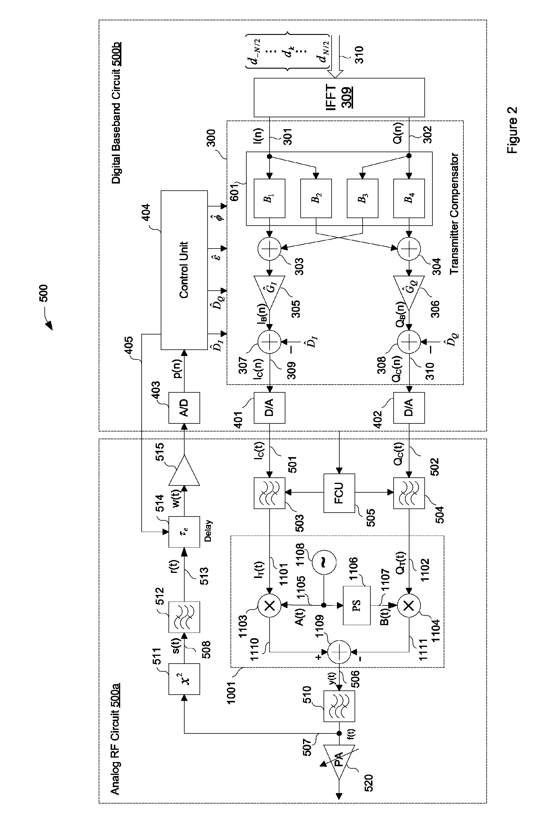
[0035]Referring to FIG. 2, a block diagram of a transmitter 500 is depicted. The transmitter 500 may include an analog RF circuit 500a and a digital baseband circuit 500b. A pair of analog baseband input signals 501 and 502, referred to herein as the inphase signal IC(t) and the quadrature signal QC(t), may enter the analog RF circuit 500a from the digital baseband circuit 500b. The inphase signal IC(t) may be supplied to a lowpass reconstruction filter 503, thereby producing an inphase signal IT(t) 1101. The inphase signal IT(t) may be used to modulate an inphase carrier signal A(t) 1105 supplied by local oscillator 1108. This modulation may be achieved by multiplying the inphase signal IT(t) and the inphase carrier signal A(t) in a first mixer 1103.

[0036]Similarly, the quadrature signal QC(t) may be supplied to a lowpass reconstruction filter 504, thereby producing a quadrature signal QT(t) 1102. The quadrature signal QT(t) may be used to modulate a quadrature carrier signal B(t) ...


PUM


Abstract

A method for correcting gain imbalance error, phase imbalance error and DC offset errors in a transmitter having an OFDM-based I / Q modulator is disclosed. The method employs a compensator prior to the I / Q-modulator to compensate for the gain and phase imbalance and DC offset. The compensator is efficiently updated with the estimated values of gain and phase imbalance and DC offsets obtained by performing the DFT operation in the digital baseband domain while sending a pair of orthogonal test tones to the modulator's inputs from a digital baseband chip, then down converting the RF modulated signal through a nonlinear device and a bandpass filter to a baseband signal, and finally sampling it using an A / D. The delay mismatch, which is mainly generated by lowpass filters between the I and Q branches, is also minimized in this method.

Description

FIELD OF THE INVENTION[0001]The invention relates to a system and method for efficiently compensating for the errors such as gain imbalance, phase imbalance and DC offset in a transmitter having a quadrature modulator.DESCRIPTION OF THE RELATED ART[0002]In digital communication systems, information to be transmitted in quadrature modulation architecture is generally split into two data sequences using a serial-to-parallel converter. One of the data sequences is provided to an inphase (I) branch and the other is provided to a quadrature (Q) branch. The data sequences on the I and Q branches are then pulse shaped or lowpass filtered to form band-limited baseband signals with spectral efficiency. The I and Q baseband signals separately modulate the phases or amplitudes of a pair of orthogonal carrier signals to realize the spectrum transfer from the baseband domain to the radio frequency (RF) domain to enable effective transmission through an antenna. In more detail, the quadrature mod...

Claims


Application Information

Patent Timeline
Patent Type & Authority Patents(United States)
IPC IPC(8): H04K1/02H04L25/03H04L25/49G06F1/04H04L27/00H03K7/00
CPCH04L25/061H04L27/2626H04L2027/0016H04L2027/0018
Inventor GAO, WEIGSHIH, DIDMIN
Owner VIA TECH INC
Why Eureka
Try Eureka