Compensation for gain imbalance, phase imbalance and DC offsets in a transmitter
- Summary
- Abstract
- Description
- Claims
- Application Information
AI Technical Summary
Benefits of technology
Problems solved by technology
Method used
Image
Examples
Embodiment Construction
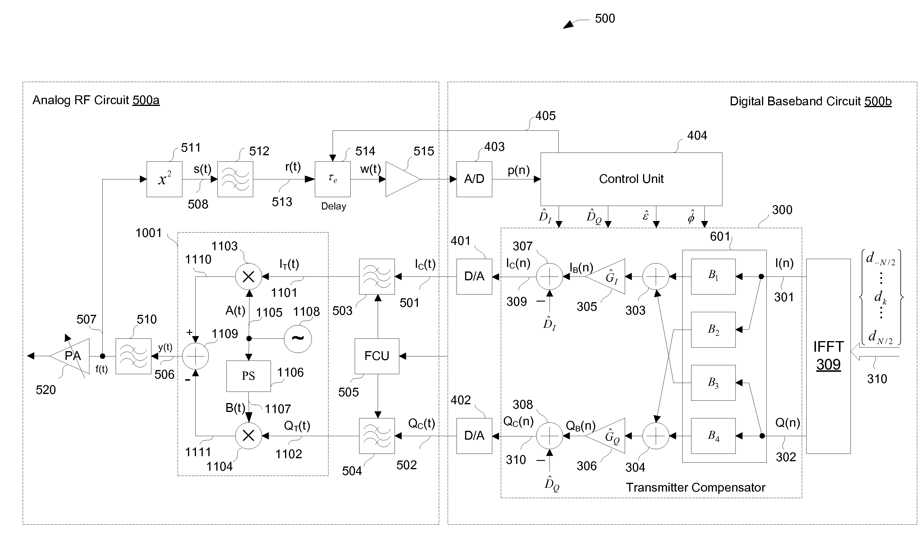
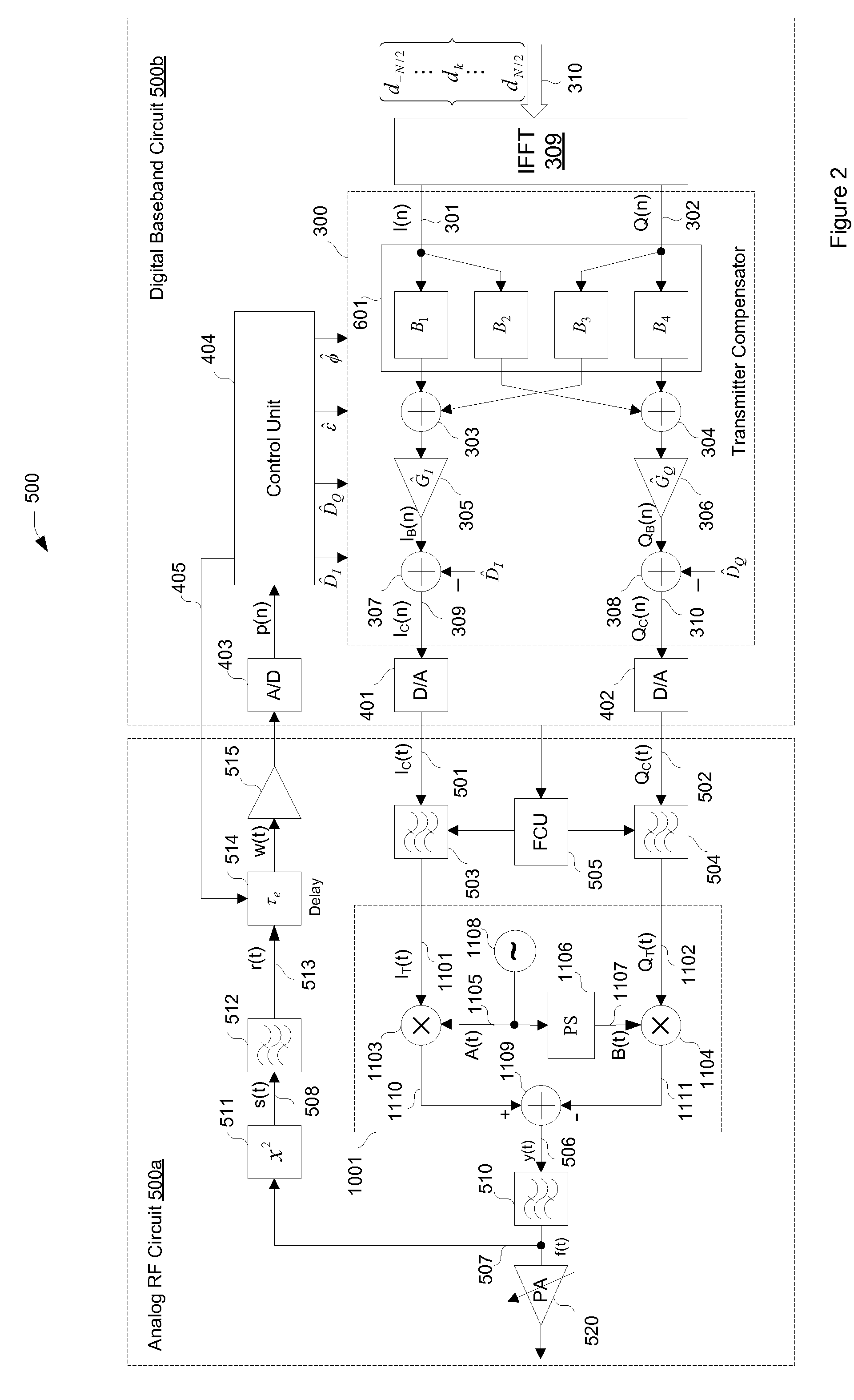
[0035]Referring to FIG. 2, a block diagram of a transmitter 500 is depicted. The transmitter 500 may include an analog RF circuit 500a and a digital baseband circuit 500b. A pair of analog baseband input signals 501 and 502, referred to herein as the inphase signal IC(t) and the quadrature signal QC(t), may enter the analog RF circuit 500a from the digital baseband circuit 500b. The inphase signal IC(t) may be supplied to a lowpass reconstruction filter 503, thereby producing an inphase signal IT(t) 1101. The inphase signal IT(t) may be used to modulate an inphase carrier signal A(t) 1105 supplied by local oscillator 1108. This modulation may be achieved by multiplying the inphase signal IT(t) and the inphase carrier signal A(t) in a first mixer 1103.
[0036]Similarly, the quadrature signal QC(t) may be supplied to a lowpass reconstruction filter 504, thereby producing a quadrature signal QT(t) 1102. The quadrature signal QT(t) may be used to modulate a quadrature carrier signal B(t) ...
PUM
 Abstract
Description
Claims
Application Information


