Supercharge Your Innovation With Domain-Expert AI Agents!

Waveguide film cable

a film cable and waveguide technology, applied in the field of waveguide film cable, can solve the problems of severed waveguide and impaired optical properties, and achieve the effect of preventing or reducing microscopic abrasion and improving flex resistan

Inactive Publication Date: 2011-02-08
MITSUMI ELECTRIC CO LTD
View PDF20 Cites 0 Cited by
  • Summary
  • Abstract
  • Description
  • Claims
  • Application Information

AI Technical Summary

Benefits of technology

[0011]According to the present invention, microscopic abrasion can be prevented or reduced, and flex resistance can be improved by the coating film.

Problems solved by technology

However, since a waveguide composed of a clad and a core is formed in the waveguide film cable, when microscopic abrasion is caused, optical properties are impaired.
In addition, when the waveguide film cable is broken, the waveguide is severed.

Method used


Image

  • Waveguide film cable
  • Waveguide film cable
  • Waveguide film cable

Examples


first modification example

[0061]FIG. 4 is a perspective view of a waveguide film cable according to a first modification example. FIG. 5 is a cross-sectional view of the waveguide film cable according to the first modification example.

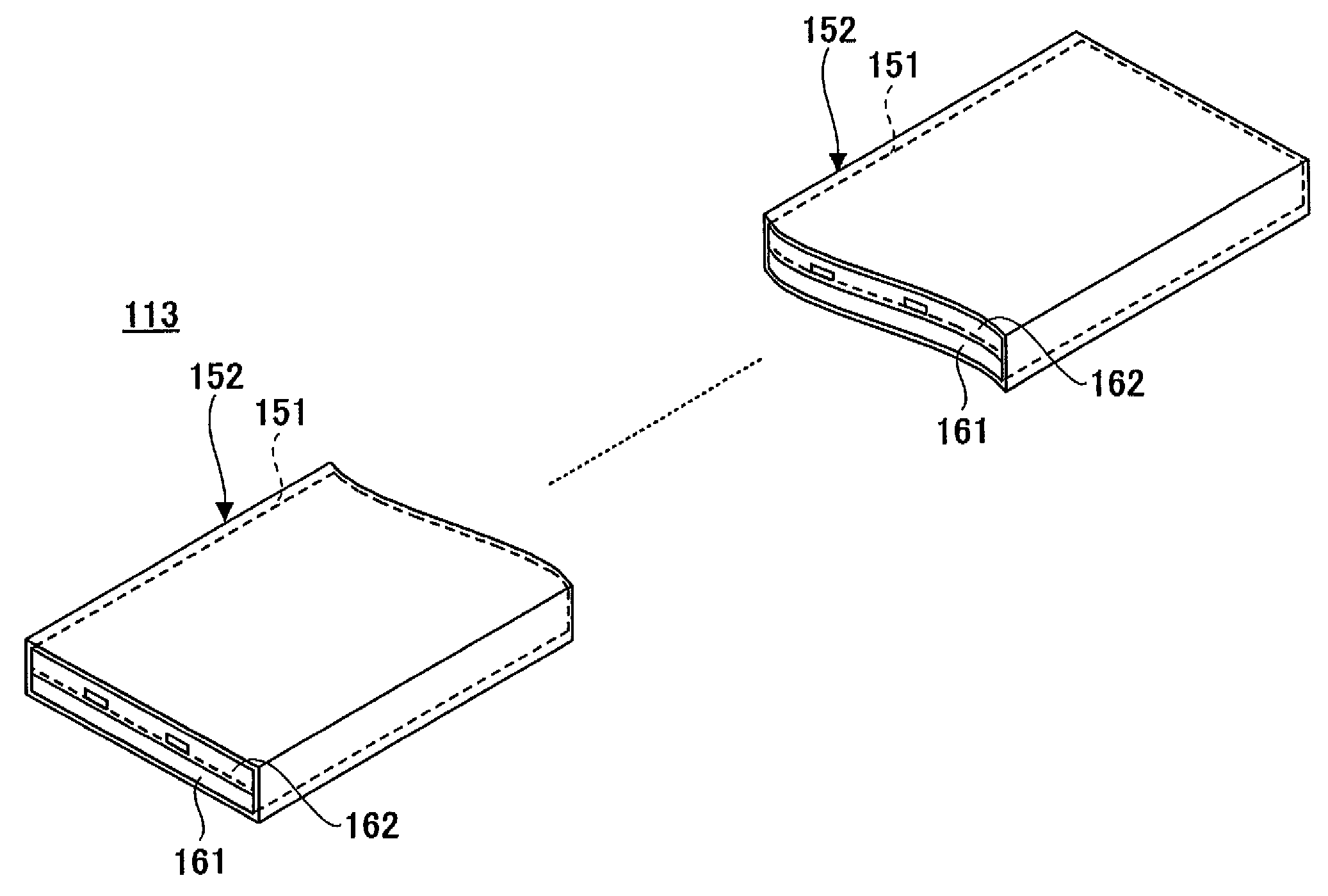
[0062]A waveguide film cable 211 according to this modification example is configured so as to include a coating film 212 only on the waveguide-formed surface of the cable body 151.

[0063]The coating film 212 formed on the waveguide-formed surface of the cable body 151 is especially effective in the flex resistance when the cable body 151 is bent so that the waveguide-formed surface makes an inner circumference.

[0064]By the way, while the coating film 212 is formed on the waveguide-formed surface (the upper surface) , the coating film 212 may be formed on the waveguide-unformed surface. The coating film 212 formed on the waveguide-unformed surface is especially effective in the flex resistance when the cable body 151 is bent so that the waveguide-unformed surface makes an inner ...

second modification example

[0065]FIG. 6 is a perspective view of a waveguide film cable according to a second modification example. FIG. 7 is a cross-sectional view of the waveguide film cable according to the second modification example.

[0066]A waveguide film cable 311 according to this modification example is configured so that a coating film 312 is formed on both side surfaces of the cable body 151.

[0067]The coating film 312 is formed by, for example, a dipping method or a stamping method. With this, the coating film 312 is formed on the waveguide-formed surface, a top peripheral portion, the waveguide-unformed surface, and a bottom peripheral portion of the cable body 151. This can alleviate stress applied to the edge faces and the peripheral portions where cracks may be easily caused.

[0068]In addition, compared to when the coating film is entirely formed on the waveguide-formed surface, optical degradation can be reduced.

third modification example

[0069]FIG. 8 is a perspective view of a waveguide film cable according to a third modification example. FIG. 9 is a cross-sectional view of the waveguide film cable according to the third modification example.

[0070]A waveguide film cable 411 is configured so as to include a cover 412 that covers the cable body 151, and a coating film 413 between the cable body 151 and the cover 412. The coating film 413 can absorb stress caused between the cover 412 and the cable body 151.


PUM


Abstract

A disclosed waveguide film cable includes a waveguide formed on a film. The waveguide film cable includes a coating film made of a material having a Young's modulus smaller than or equal to the Young's modulus of a material that forms the film and / or the waveguide and coats partially or entirely the film and / or the waveguide.

Description

TECHNICAL FIELD[0001]The present invention relates to a waveguide film cable, specifically to a waveguide film cable that includes a waveguide formed on a film.BACKGROUND ART[0002]With a recent advancement of optical fiber networks, optical fiber is being introduced into residences. Light from the optical fiber is supplied to an optical module or an optical interconnection board, and then branched so as to be supplied into appliances having an optical input.[0003]The optical module or the optical interconnection board having an optical circuit, a photo-detector, and a light emitting device are optically coupled by a waveguide film cable that enables optical interconnection.[0004]In order to enhance degrees of freedom in arrangement of the optical modules or the optical interconnect boards, enhanced degrees of freedom in bending the waveguide film cable have been desired. However, since a waveguide composed of a clad and a core is formed in the waveguide film cable, when microscopic ...

Claims


Application Information

Patent Timeline
Patent Type & Authority Patents(United States)
IPC IPC(8): G02B6/10
CPCG02B6/10G02B6/1221G02B6/42G02B6/4401G02B6/02033G02B6/02042G02B6/43G02B6/44
Inventor ONO, TADASHI
Owner MITSUMI ELECTRIC CO LTD
Features
  • R&D
  • Intellectual Property
  • Life Sciences
  • Materials
  • Tech Scout
  • Unparalleled Data Quality
  • Higher Quality Content
  • 60% Fewer Hallucinations
Learn More