Semiconductor light-emitting device and method for making same

a technology of semiconductors and light-emitting devices, applied in the field of semiconductor light-emitting devices, can solve the problems of electrodes obstructing a substantial amount of vertically emitted light, high light-emission efficiency, and particularly pronounced light-obstruction issues, and achieve the effect of reducing the recombination of carriers

Active Publication Date: 2011-04-05
LATTICE POWER (JIANGXI) CORP
View PDF10 Cites 2 Cited by
  • Summary
  • Abstract
  • Description
  • Claims
  • Application Information

AI Technical Summary

Benefits of technology

[0010]In a variation of this embodiment, the shape of the lower ohmic-contact layer is substantially complementary to the shape of the upper ohmic-contact layer, thereby allowing the carrier flow to be concentrated in the portion of the active layer where light emitted upward is not substantially obstructed by the upper ohmic-contact layer.
[0014]In a variation of this embodiment, the device further includes a layer of high-resistance material situated between the lower cladding layer and the lower ohmic-contact layer. The high-resistance material is confined to a region substantially below the upper ohmic-contact layer, thereby reducing carrier recombination occurring below the upper ohmic-contact layer which can obstruct light emitted upward.
[0016]A further embodiment of the present invention provides a semiconductor light-emitting device, which comprises: an upper cladding layer, a lower cladding layer, an active layer between the upper and lower cladding layers, an upper ohmic-contact layer forming a conductive path to the upper cladding layer, and a lower ohmic-contact layer forming a conductive path to the lower cladding layer. Furthermore, a portion of the lower cladding layer, or a portion of the active layer, or both, is not present at a region substantially below the upper ohmic-contact layer, thereby reducing carrier recombination below the upper ohmic-contact layer which causes light emitted upward to be obstructed by the upper ohmic-contact layer.

Problems solved by technology

Higher light-emission efficiency, like for conventional incandescent or florescent lights, remains a challenge for LED designers.
The light-obstruction issue is particularly pronounced in an LED with a vertical-electrode structure, that is, the entire device is situated between an upper and lower electrodes.
When a significant overlap exists between the upper and lower electrodes, the electrodes can obstruct a substantial amount of vertically emitted light.
The concentration of carriers in this undesirable location further exacerbates the vertical-light obstruction problem.

Method used


Image

  • Semiconductor light-emitting device and method for making same
  • Semiconductor light-emitting device and method for making same
  • Semiconductor light-emitting device and method for making same

Examples


Embodiment Construction

[0038]The following description is presented to enable any person skilled in the art to make and use the invention, and is provided in the context of a particular application and its requirements. Various modifications to the disclosed embodiments will be readily apparent to those skilled in the art, and the general principles defined herein may be applied to other embodiments and applications without departing from the scope of the present invention. Thus, the present invention is not limited to the embodiments shown, but is to be accorded the widest scope consistent with the claims.

Obstruction of Vertically Emitted Light

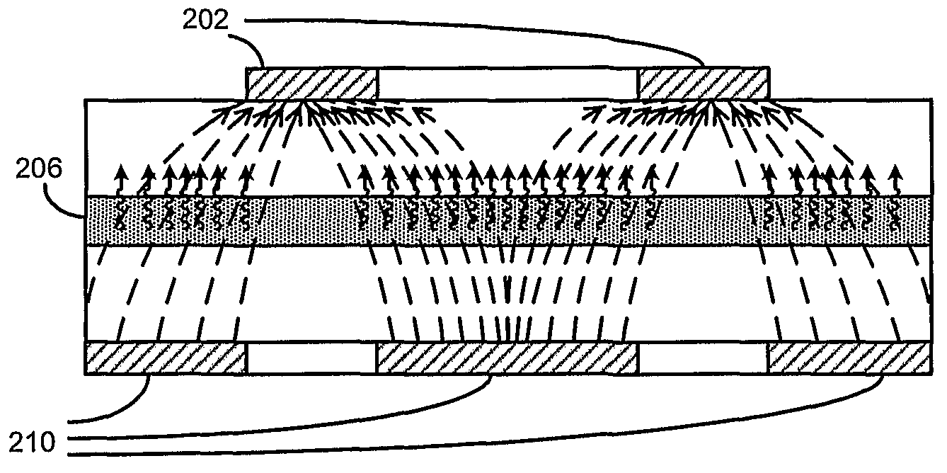
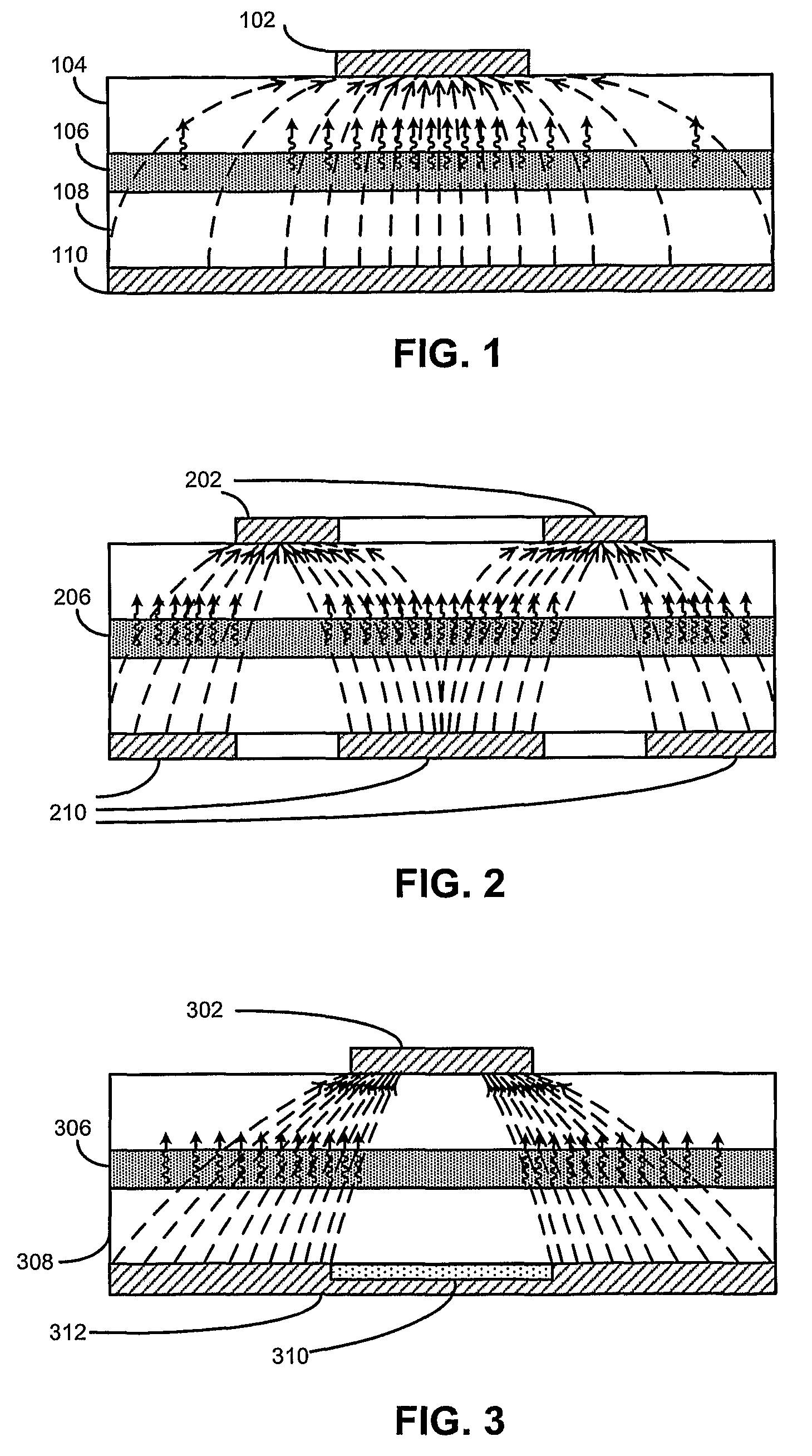
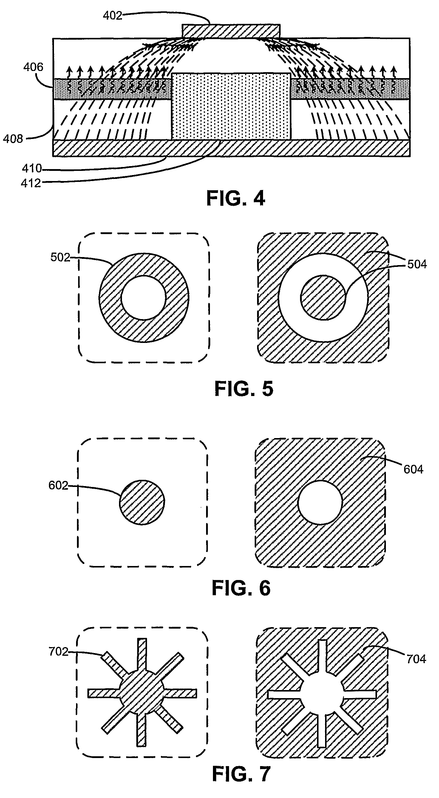
[0039]Generally, the two electrode of an LED can be placed on the same side of the substrate (lateral electrodes) or on different sides of the substrate (vertical electrodes). Vertical-electrode configuration is a preferred design due to its ease of packaging and better reliability. FIG. 1 illustrates a typical LED structure with vertical electrodes.

[0040]An active...


PUM


Abstract

One embodiment of the present invention provides a semiconductor light-emitting device, which comprises: an upper cladding layer; a lower cladding layer; an active layer between the upper and lower cladding layers; an upper ohmic-contact layer forming a conductive path to the upper cladding layer; and a lower ohmic-contact layer forming a conductive path the lower cladding layer. The lower ohmic-contact layer has a shape substantially different from the shape of the upper ohmic-contact layer, thereby diverting a carrier flow away from a portion of the active layer which is substantially below the upper ohmic-contact layer when a voltage is applied to the upper and lower ohmic-contact layers.

Description

BACKGROUND[0001]1. Field of the Invention[0002]The present invention relates to the design of semiconductor light-emitting devices. More specifically, the present invention relates to novel device structures which facilitate more efficient light emission.[0003]2. Related Art[0004]Solid-state lighting is expected to be the illumination wave of the future. High-brightness light-emitting diodes (HB-LEDs) are beginning to penetrate an increasing number of applications, especially as the light source for display devices and as light-bulb replacement for conventional lighting. Higher light-emission efficiency, like for conventional incandescent or florescent lights, remains a challenge for LED designers.[0005]An LED typically produces light from an active region which is situated between a positively-doped cladding layer (p-type cladding layer) and negatively-doped cladding layer (n-type cladding layer). When the LED is forward-biased, the carriers, which include holes from the p-type cla...

Claims


Application Information

Patent Timeline
Patent Type & Authority Patents(United States)
IPC IPC(8): H01L33/00H01L33/06H01L33/10H01L33/32H01L33/38H01L33/40
CPCH01L33/145H01L33/40H01L33/0079H01L2933/0016H01L33/38H01L33/32H01L33/0093
Inventor JIANG, FENGYIWANG, LIFANG, WENQING
Owner LATTICE POWER (JIANGXI) CORP
Why Eureka
Try Eureka