Photoelectric conversion device
- Summary
- Abstract
- Description
- Claims
- Application Information
AI Technical Summary
Benefits of technology
Problems solved by technology
Method used
Image
Examples
embodiment 1
[0037]In this embodiment, a photoelectric conversion device according to one embodiment of the present invention and a method for manufacturing the photoelectric conversion device will be described.
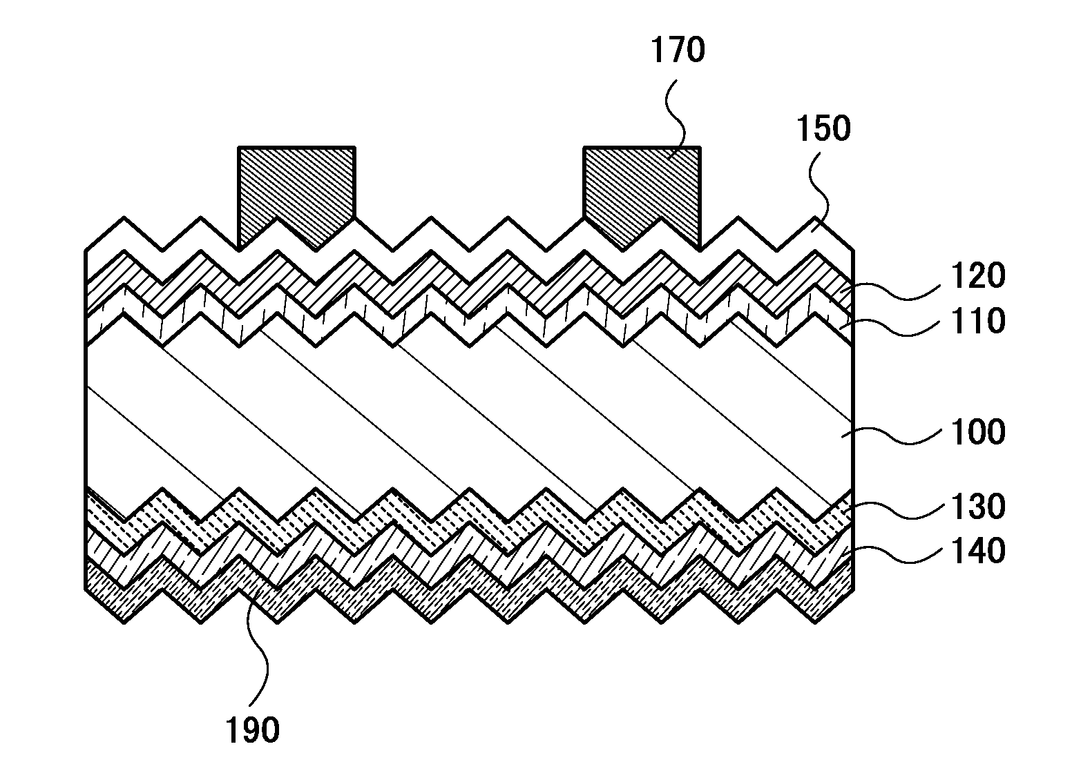
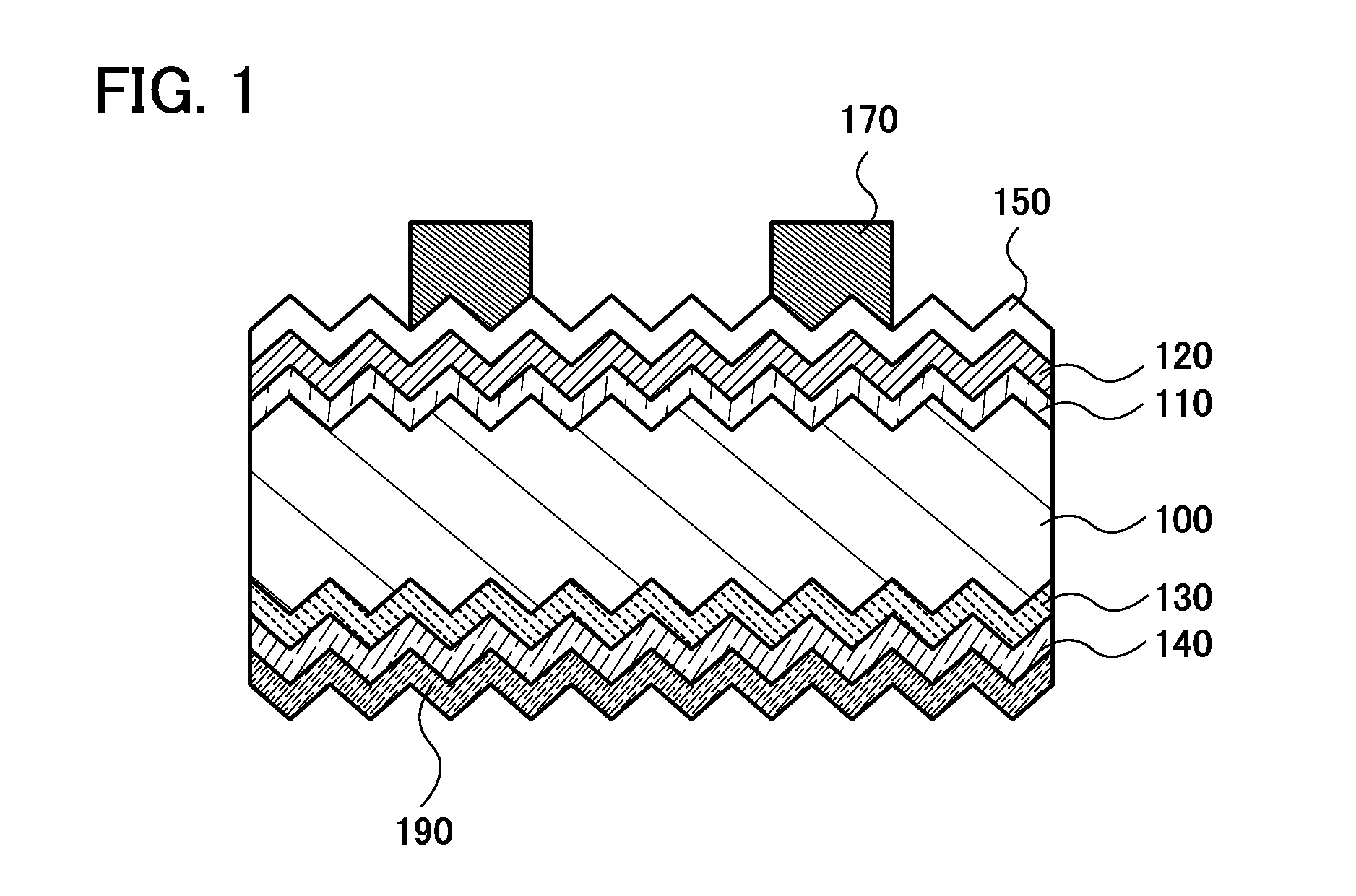
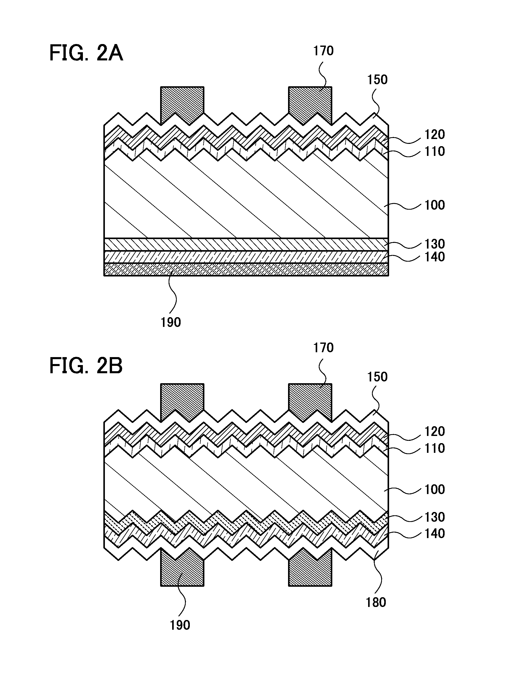
[0038]FIG. 1 is a cross-sectional view of a photoelectric conversion device according to one embodiment of the present invention. The photoelectric conversion device includes a crystalline silicon substrate 100 whose surfaces are processed to have unevenness and further includes, over one surface of the crystalline silicon substrate, a first silicon semiconductor layer 110, a second silicon semiconductor layer 120, a light-transmitting conductive film 150, and a first electrode 170. Furthermore, the photoelectric conversion device includes a third silicon semiconductor layer 130 provided on the other surface of the crystalline silicon substrate, a fourth silicon semiconductor layer 140 provided on the third silicon semiconductor layer 130, and a second electrode 190 provided on the fourth...
embodiment 2
[0086]In this embodiment, a photoelectric conversion device having a structure which is different from that described in Embodiment 1 is described. Note that detailed description of the common portions to that in Embodiment 1 is omitted in this embodiment.
[0087]FIG. 5 is a cross-sectional view of a photoelectric conversion device according to one embodiment of the present invention. The photoelectric conversion device includes a crystalline silicon substrate 200 whose surfaces are processed to have unevenness and further includes, over one surface of the crystalline silicon substrate, a first silicon semiconductor layer 210, a light-transmitting conductive film 250, and a first electrode 270. Furthermore, the photoelectric conversion device includes a second silicon semiconductor layer 220 provided on the other surface of the crystalline silicon substrate and a second electrode 290 provided on the second silicon semiconductor layer 220. Note that the first electrode 270 is a grid el...
example 1
[0111]In this example, comparison evaluation results of lifetimes for studying a passivation effect of various p-type and n-type silicon semiconductor layers are described.
[0112]FIG. 9 is a cross-sectional view of a sample for measurement of the lifetime. As a substrate 300, an n-type single crystal silicon substrate (with a diameter of 2 inches, a thickness of 300 μm, and a resistivity of 1000 Ω·cm or higher) formed by an FZ method was used. Further, as a first passivation layer 310, any one of an i-type silicon semiconductor layer, a p-type silicon semiconductor layer, or an n-type silicon semiconductor layer was used. In addition, the thickness was 5 nm. Furthermore, as a second passivation layer 320, an i-type silicon semiconductor layer was used and the thickness was 15 nm. Note that a plurality of samples was manufactured so as to obtain a different electrical conductivity.
[0113]Any p-type silicon semiconductor layer was formed by a manufacturing method similar to that in Embo...
PUM
 Abstract
Description
Claims
Application Information


