Process for making dense thin films

a thin film, dense technology, applied in the manufacture of cell components, final product manufacturing, electrochemical generators, etc., can solve the problems of high cost, low electronic conductivity of lsm substrate, and insufficient electronic conductivity of high-efficiency current collection, so as to reduce resistive losses in the device, high electronic conductivity, and high strength

Inactive Publication Date: 2005-07-26
RGT UNIV OF CALIFORNIA
View PDF57 Cites 21 Cited by
  • Summary
  • Abstract
  • Description
  • Claims
  • Application Information

AI Technical Summary

Benefits of technology

[0014]In general, the present invention provides low-cost, mechanically strong, porous structures for a variety of uses, techniques for forming these structures, and devices incorporating the structures. In preferred embodiments, the invention provides a porous electrode designed for high strength and high electronic conductivity (to lower resistive losses in the device due to current collection). Conventional Ni-YSZ based SOFCs may be greatly improved by application of the present invention by, for example, casting a thin layer of Ni-YSZ on top of a porous high-strength alloy support—this also substantially lowers the cost of the device by using inexpensive alloy material for mechanical strength as opposed to nickel. Alternatively, alloys known to have good oxidation resistance can be used to form a high-strength electrode in a solid state electrochemical device. In this embodiment, an alloy such as Inconel 600 is used to make a porous high-strength electrode onto which an electrolyte membrane is co-fired.

Problems solved by technology

However, in the existing design the support is pre-fired porous LSM onto which the YSZ coating is applied by CVD-EVD, a very expensive process.
Also, the LSM substrate does not have sufficient electronic conductivity for highly efficient current collection.

Method used


Image

  • Process for making dense thin films
  • Process for making dense thin films
  • Process for making dense thin films

Examples


Embodiment Construction

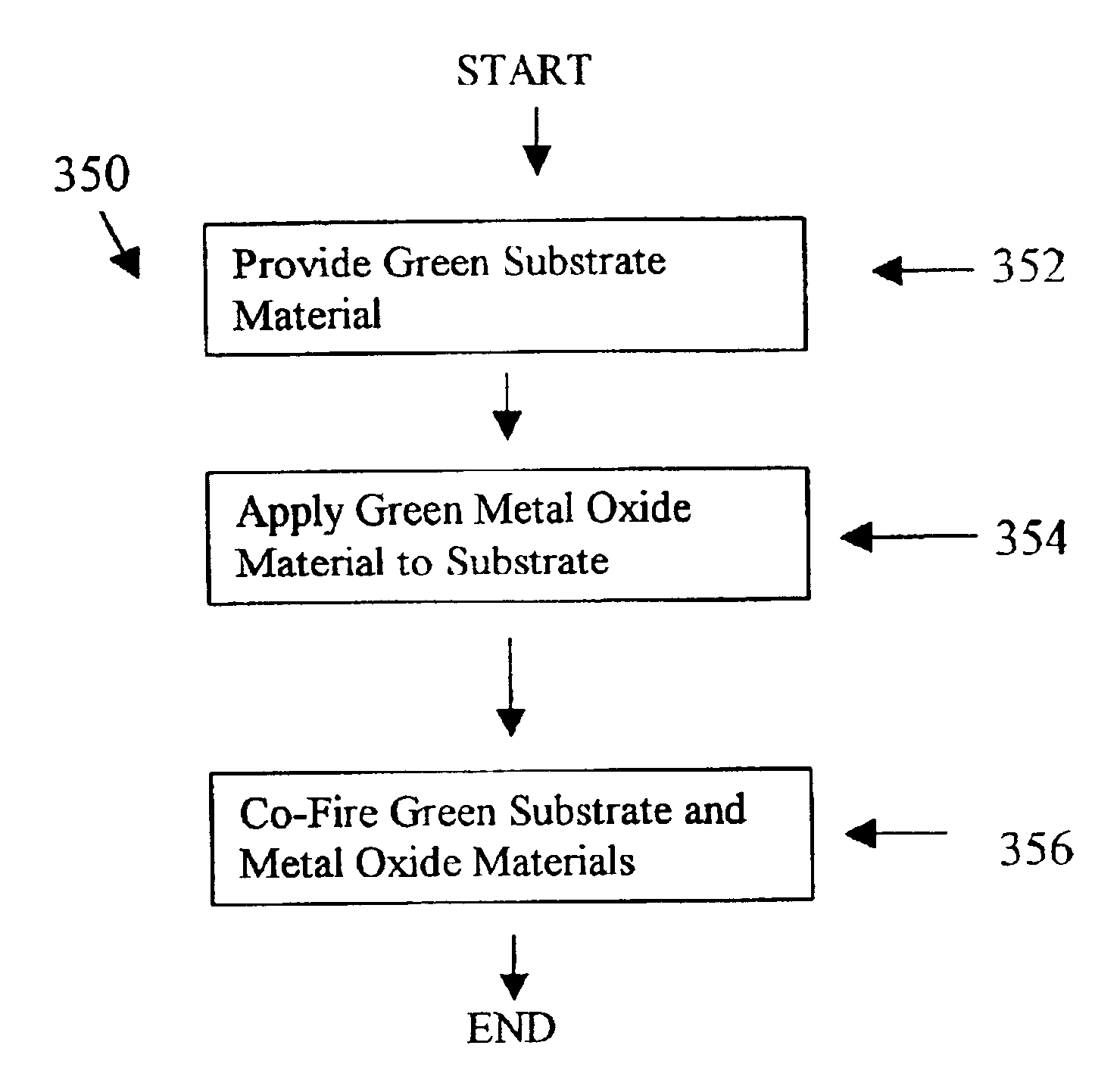
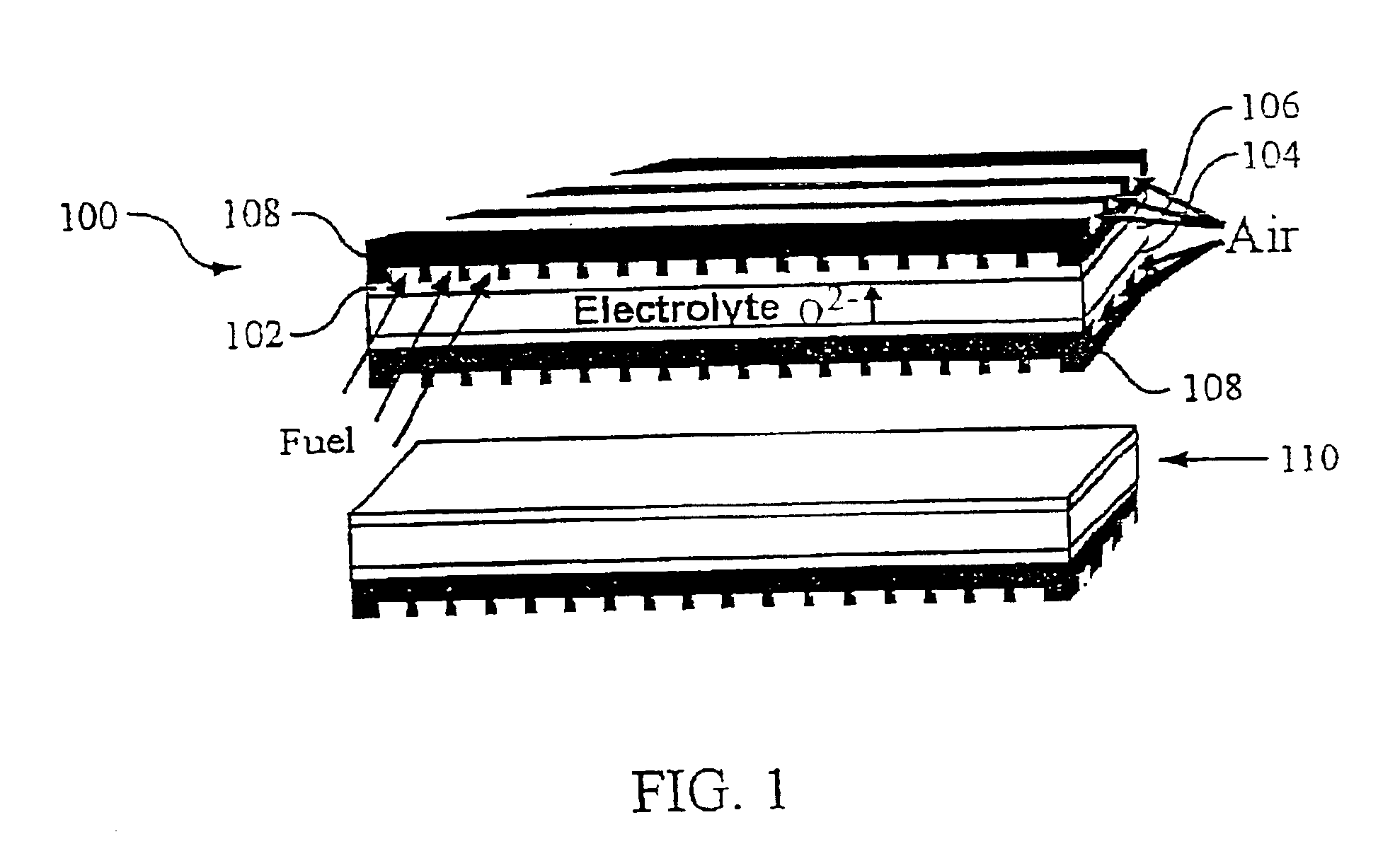
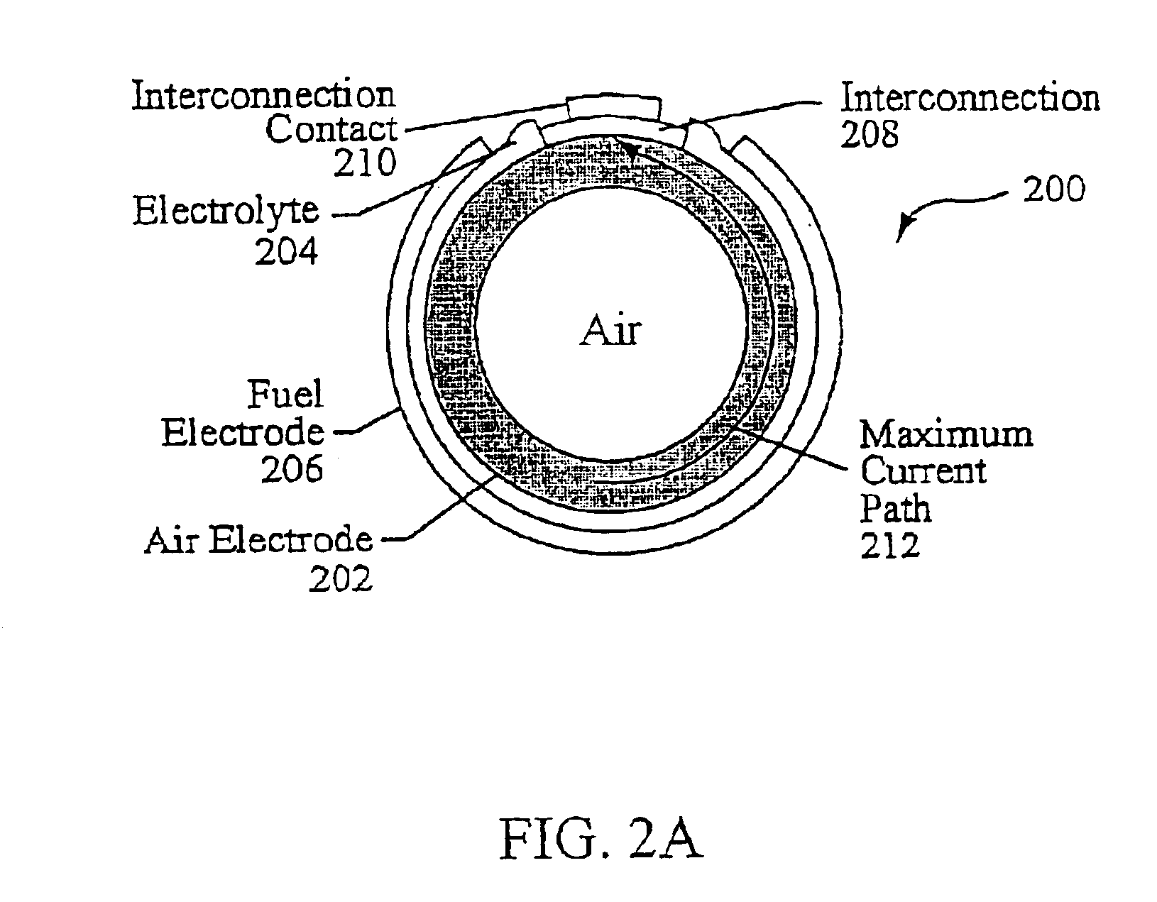
[0025]Reference will now be made in detail to some specific embodiments of the invention including the best modes contemplated by the inventors for carrying out the invention. Examples of these specific embodiments are illustrated in the accompanying drawings. While the invention is described in conjunction with these specific embodiments, it will be understood that it is not intended to limit the invention to the described embodiments. On the contrary, it is intended to cover alternatives, modifications, and equivalents as may be included within the spirit and scope of the invention as defined by the appended claims. In the following description, numerous specific details are set forth in order to provide a thorough understanding of the present invention. The present invention may be practiced without some or all of these specific details. In other instances, well known process operations have not been described in detail in order not to unnecessarily obscure the present invention....


PUM

PropertyMeasurementUnit
temperatureaaaaaaaaaa
particle sizeaaaaaaaaaa

Abstract

Provided are low-cost, mechanically strong, highly electronically conductive porous substrates and associated structures for solid-state electrochemical devices, techniques for forming these structures, and devices incorporating the structures. The invention provides solid state electrochemical device substrates of novel composition and techniques for forming thin electrode/membrane/electrolyte coatings on the novel or more conventional substrates. In particular, in one embodiment the invention provides techniques for firing of device substrate to form densified electrolyte/membrane films 5 to 20 microns thick. In another embodiment, densified electrolyte/membrane films 5 to 20 microns thick may be formed on a pre-sintered substrate by a constrained sintering process. In some cases, the substrate may be a porous metal, alloy, or non-nickel cermet incorporating one or more of the transition metals Cr, Fe, Cu and Ag, or alloys thereof.

Description

CROSS REFERENCE TO RELATED APPLICATIONS[0001]This applications claims priority to U.S. Ser. No. 60 / 343,294, filed Dec. 18, 2001, the contents which are hereby incorporated by reference in their entirety for all purposes.STATEMENT REGARDING FEDERALLY SPONSORED RESEARCH OR DEVELOPMENT[0002]This invention was made with government support under Grant (Contract) No. DE-AC03-76F00098 awarded by The United States Department of Energy. The government has certain rights to this invention.BACKGROUND OF THE INVENTION[0003]The present invention relates generally to the field of solid state electrochemical devices, and more particularly to substrate, electrode and cell structures for solid state electrochemical devices.[0004]Solid state electrochemical devices are often implemented as cells including two porous electrodes, the anode and the cathode, and a dense solid electrolyte and / or membrane which separates the electrodes. For the purposes of this application, unless otherwise explicit or cle...

Claims


Application Information

Patent Timeline
Patent Type & Authority Patents(United States)
IPC IPC(8): B05D1/36B05D3/02H01M8/12
CPCH01M8/1213H01M8/1226H01M4/9066H01M8/1246Y02E60/521Y02E60/525Y02E60/50Y02P70/50
Inventor JACOBSON, CRAIG P.VISCO, STEVEN J.DEJONGHE, LUTGARD C.
Owner RGT UNIV OF CALIFORNIA
Why Eureka
Try Eureka