Liquid crystal display device and manufacturing method thereof

a technology of liquid crystal display and manufacturing method, which is applied in non-linear optics, instruments, optics, etc., can solve the problems of information leakage to persons, infringement of private life of users, misalignment, etc., and achieve the effect of convenient security and high quality imag

Inactive Publication Date: 2011-05-10
LG DISPLAY CO LTD
View PDF14 Cites 10 Cited by
  • Summary
  • Abstract
  • Description
  • Claims
  • Application Information

AI Technical Summary

Benefits of technology

[0026]An object of the present invention is to provide a liquid crystal display device that allows an excellent image quality even at a wide viewing angle and controls a viewing angle depending on a user's selection to allow an image to be viewed only at a narrow viewing angle.
[0030]The present invention provides flexibility in an aspect of a security range to a user. According to the present invention, an LCD device can be exclusively used for one person, and provide a high quality image and achieve security conveniently even when two or more persons view the image using the LCD device.

Problems solved by technology

For example, when an LCD device has only a wide viewing angle in the case where the LCD device is used in order to protect company secret or national secret, and private life, information may leak out to persons located at an adjacent position or private life of a user may be infringed.
Also, misalign may occur when the viewing angle controlling LC panel and the main LC panel are attached to each other.

Method used


Image

  • Liquid crystal display device and manufacturing method thereof
  • Liquid crystal display device and manufacturing method thereof
  • Liquid crystal display device and manufacturing method thereof

Examples


first embodiment

[0051]According to the present invention, each of the red subpixel Pr, green subpixel Pg, and blue subpixel Pb has a transflective structure, and the viewing angle controlling subpixel Pv has a transmissive structure.

second embodiment

[0052]According to the present invention, each of the red subpixel Pr, green subpixel Pg, and blue subpixel Pb has a transflective structure, and the viewing angle controlling subpixel Pv has a transflective structure.

[0053]An LCD device according to the present invention can be switched between a narrow viewing mode and a wide viewing angle mode by selectively controlling the viewing angle controlling subpixel Pv in an on-state and an off-state.

[0054]In an LCD device according to the present invention, the red subpixel Pr, green subpixel Pg, blue subpixel Pb, and viewing angle controlling subpixel Pv can be arranged in various shapes. For example, the red subpixel Pr, green subpixel Pg, blue subpixel Pb, and viewing angle controlling subpixel Pv can be arranged in a quad type disposed in two by two, or in a stripe type disposed in a line.

[0055]The present invention provides flexibility in an aspect of a security range to a user. According to the present invention, an LCD device can...

third embodiment

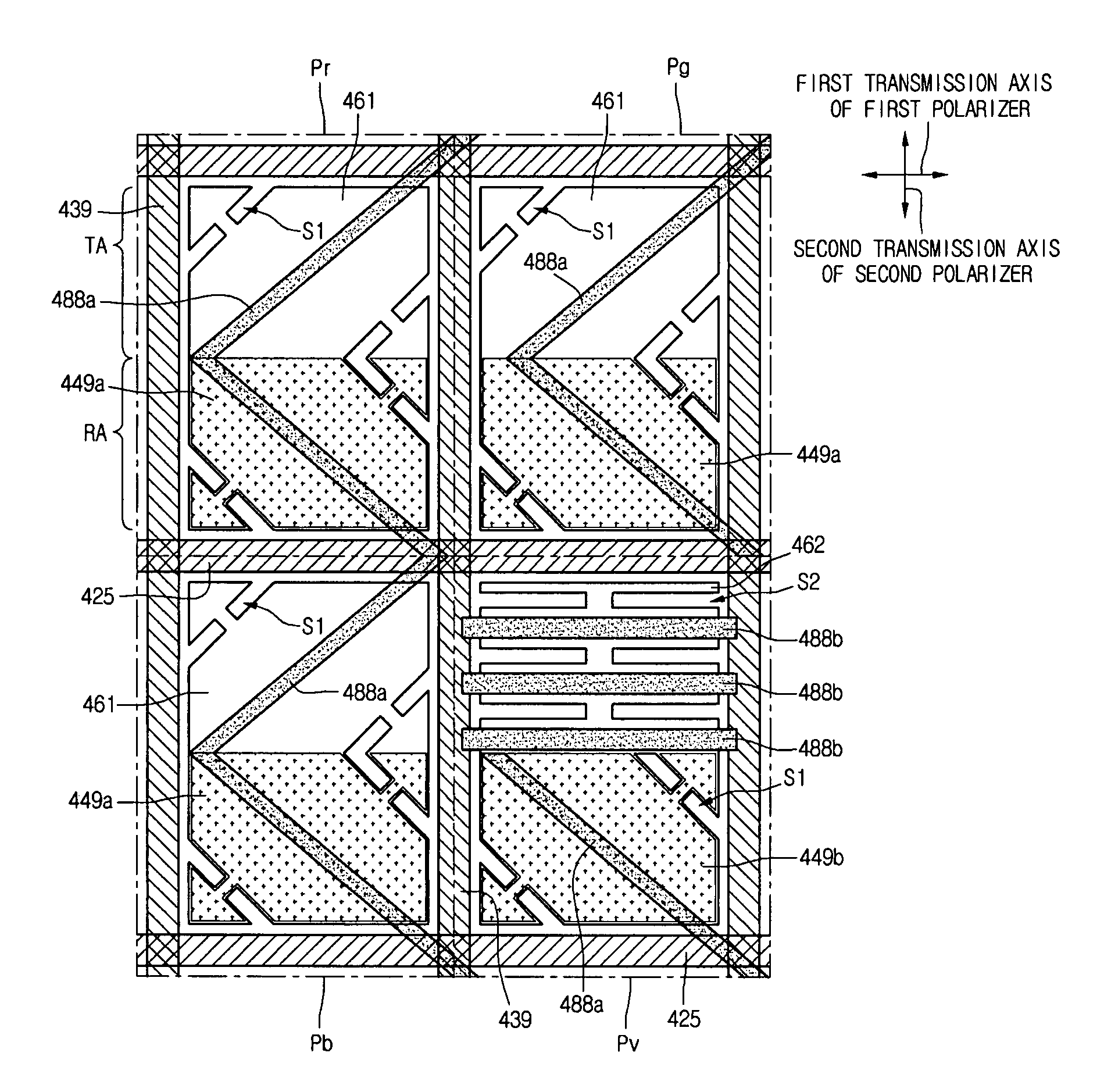
[0161]FIG. 8 is a schematic plan view illustrating a pixel of an LCD device according to the present invention.

[0162]FIG. 8 schematically illustrates electrode structures of subpixels and rib patterns, and does not illustrate a thin film transistor.

[0163]Referring to FIG. 8, a pixel of the LCD device includes a red subpixel Pr, a green subpixel Pg, a blue subpixel Pb, and a viewing angle controlling subpixel Pv by a crossing of a gate line 325 and a data line 339, and is driven in a VA mode.

[0164]A first slit S1 long in a second direction and a third direction is formed in a first pixel electrode 361 of the red subpixel Pr, green subpixel Pg, and blue subpixel Pb of the first substrate.

[0165]A first rib 388a is formed in the second and third directions on the red subpixel Pr, green subpixel Pg, and blue subpixel Pb of the second substrate.

[0166]The second direction and the third direction are perpendicular to each other. The first rib 388a and the first slit S1 are formed in a bent ...


PUM

PropertyMeasurementUnit
optical densityaaaaaaaaaa
transmittanceaaaaaaaaaa
reflection areaaaaaaaaaaa

Abstract

Provided are an LCD device that can control a viewing angle freely and a manufacturing method thereof. The LCD device includes a first substrate, a second substrate, and an LC layer interposed between the first and second substrates. The LCD device further includes red, green, blue, and viewing angle controlling subpixels. These subpixels are driven in a VA mode. The red, green, and blue subpixels have a transflective structure. The viewing angle controlling subpixel has a transmissive or transflective structure.

Description

[0001]This application claims the benefit of Korean Patent Application No. 10-2006-0126763 filed in Korea on Dec. 13, 2006, which is hereby incorporated by reference in its entirety.BACKGROUND OF THE INVENTION[0002]1. Field of the Invention[0003]The present invention relates to a liquid crystal display (LCD) device and a manufacturing method thereof.[0004]2. Description of the Related Art[0005]Recently, an LCD device, which is one of flat display devices in the limelight constantly, changes optical anisotropy by applying an electric field to liquid crystal (LC) having both fluidity of liquid and an optical property of a crystal. The LCD device has a small volume and low power consumption compared to a related art cathode ray tube (CRT), and can be manufactured in a large size and achieve high definition. Accordingly, the LCD device is widely used.[0006]The LCD device can be classified into various mode LCD devices depending on the property of the LC and a pattern structure.[0007]In ...

Claims


Application Information

Patent Timeline
Patent Type & Authority Patents(United States)
IPC IPC(8): G02F1/1335
CPCG02F1/1323G02F1/134336G02F1/133555G02F2001/134345G02F1/1393G02F1/134345G02F1/1335
Inventor JIN, HYUN SUKJANG, HYUNG SEOKKIM, TAE HAN
Owner LG DISPLAY CO LTD
Why Eureka
Try Eureka