

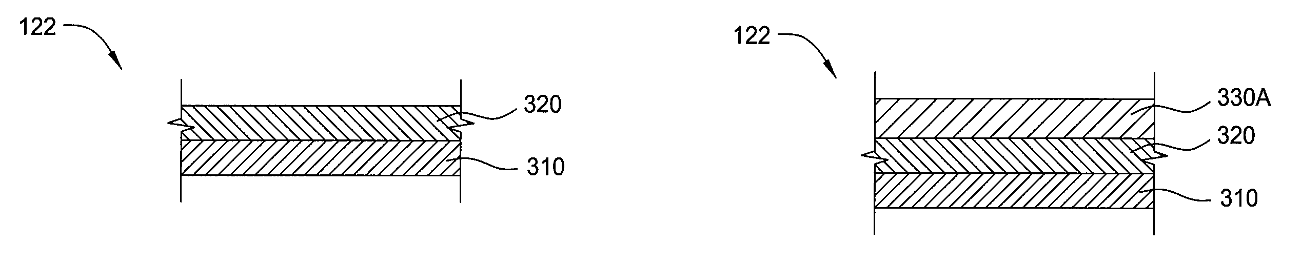
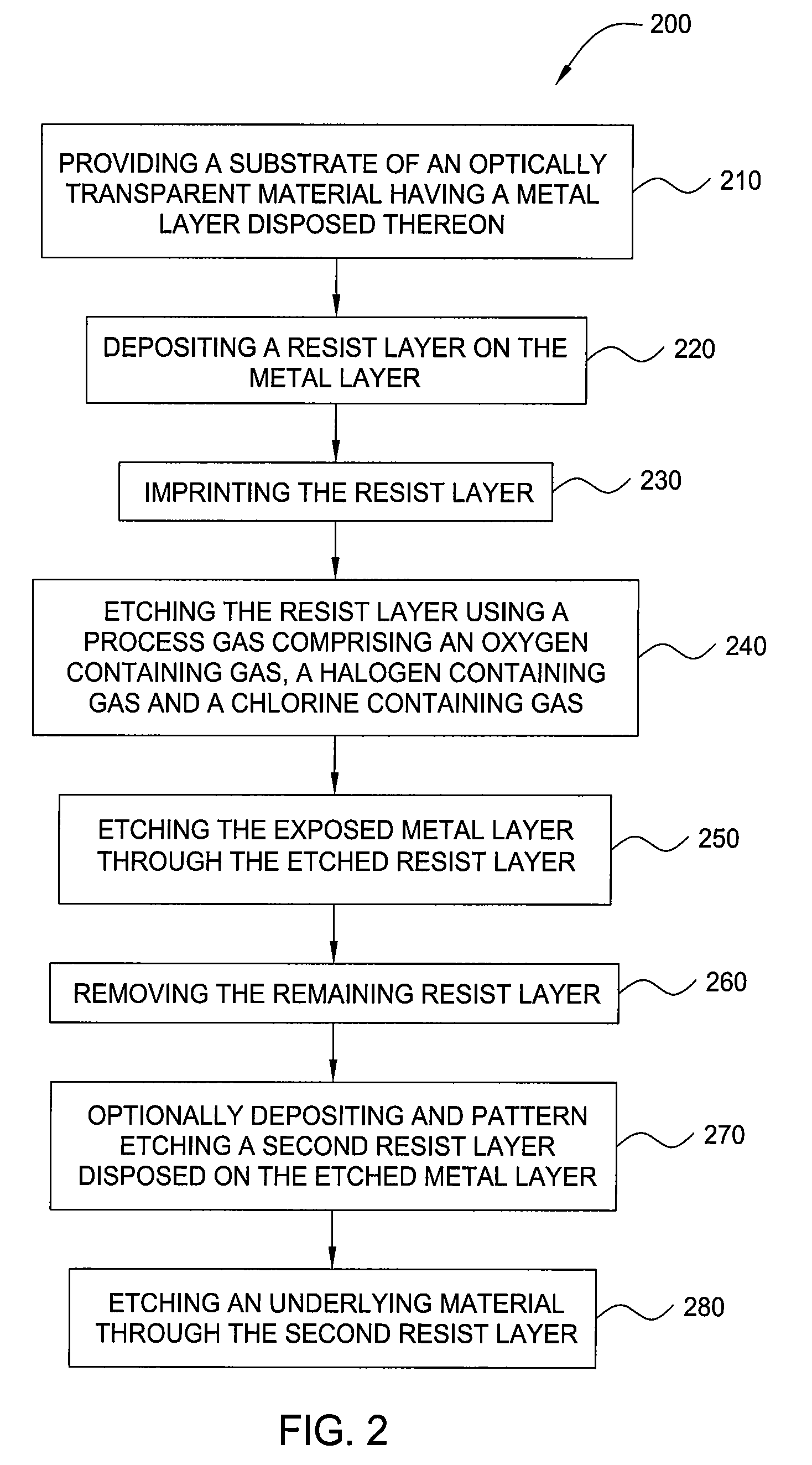
Etching of nano-imprint templates using an etch reactor
a nano-imprint and etching technology, applied in the direction of photomechanical treatment originals, instruments, photomechanical equipment, etc., can solve the problems of losing the critical dimensions of features, most conventional etching processes, and not being able to robustly transfer such small patterns to the underlying material
- Summary
- Abstract
- Description
- Claims
- Application Information
AI Technical Summary
Problems solved by technology
Method used
Image

Examples
Embodiment Construction
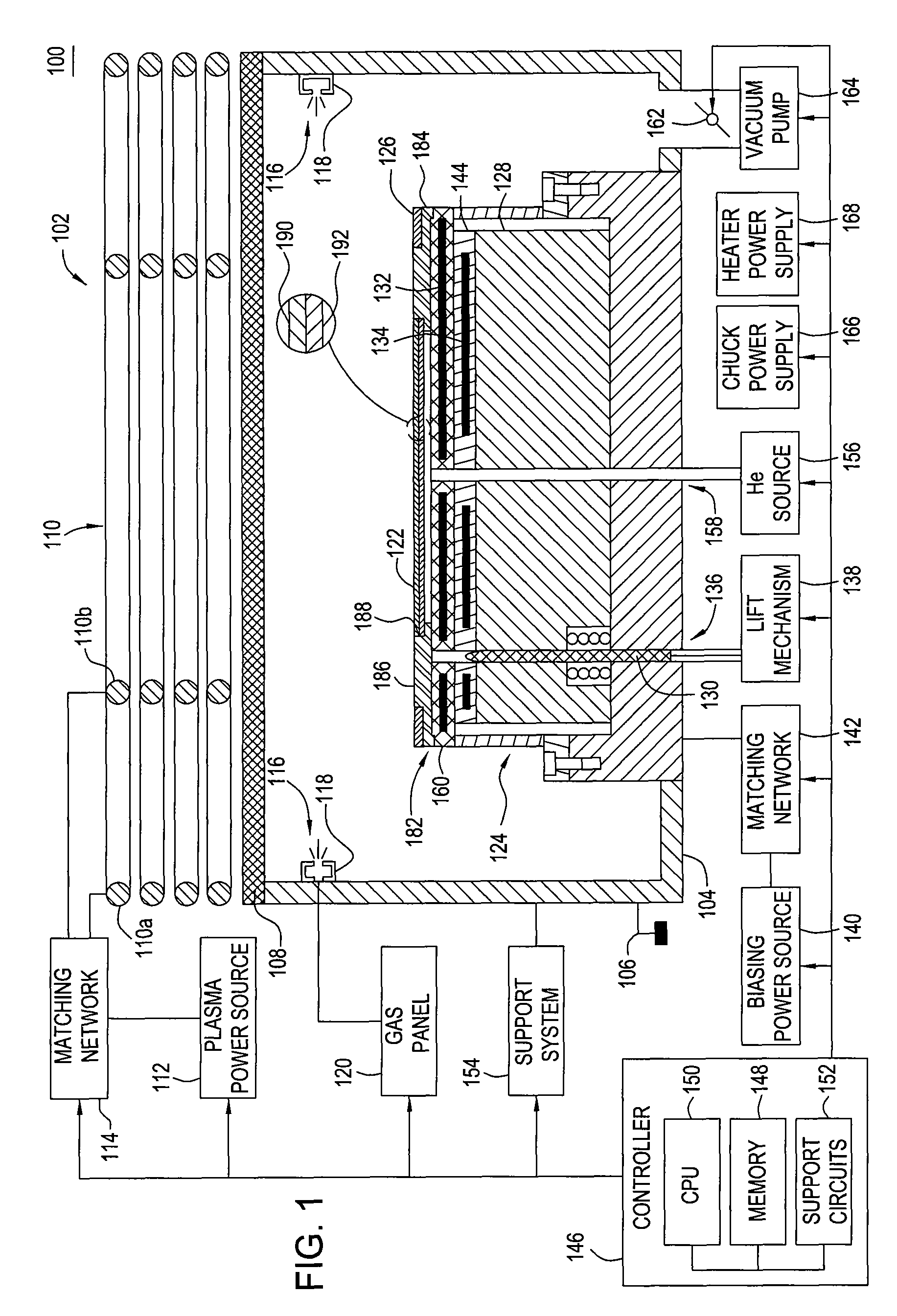
[0021]Aspects of the invention will be described below in reference to an inductively coupled plasma etch chamber. Suitable inductively coupled plasma etch chambers include the Tetra™ family of photomask etch chambers, or optionally, a Decoupled Plasma Source (DPS I™, DPS II™, and DPS Plus™) processing chambers, all available from Applied Materials, Inc., of Santa Clara, Calif.
[0022]Other process chambers may be used to perform the processes of the invention, including, for example, capacitively coupled parallel plate chambers and magnetically enhanced ion etch chambers as well as inductively coupled plasma etch chambers of different designs. Examples of such suitable processing chambers are disclosed in U.S. patent application Ser. No. 09 / 325,026, filed on Jun. 3, 1999, U.S. patent application Ser. No. 11 / 554,502, filed on Oct. 30, 2006, and in U.S. patent application Ser. No. 11 / 554,495, filed on Oct. 30, 2006, which are incorporated by reference. Although the processes are advant...
PUM
| Property | Measurement | Unit |
|---|---|---|
| frequency | aaaaa | aaaaa |
| frequency | aaaaa | aaaaa |
| pressures | aaaaa | aaaaa |
Abstract
Description
Claims
Application Information