Method for forming a one-transistor memory cell and related structure

a memory cell and one-transistor technology, applied in the field of semiconductor devices, can solve the problems of inability to meet the needs of customers,

Active Publication Date: 2011-07-05
GLOBALFOUNDRIES U S INC
View PDF8 Cites 13 Cited by
  • Summary
  • Abstract
  • Description
  • Claims
  • Application Information

AI Technical Summary

Problems solved by technology

In a conventional one-transistor DRAM cell, the sensing margin is typically too low.
As a result, the conventional one-transistor DRAM cell can require complicated sensing circuitry to distinguish a logic “1” from a logic “0,” which can undesirably increase manufacturing cost.

Method used


Image

  • Method for forming a one-transistor memory cell and related structure
  • Method for forming a one-transistor memory cell and related structure
  • Method for forming a one-transistor memory cell and related structure

Examples


Embodiment Construction

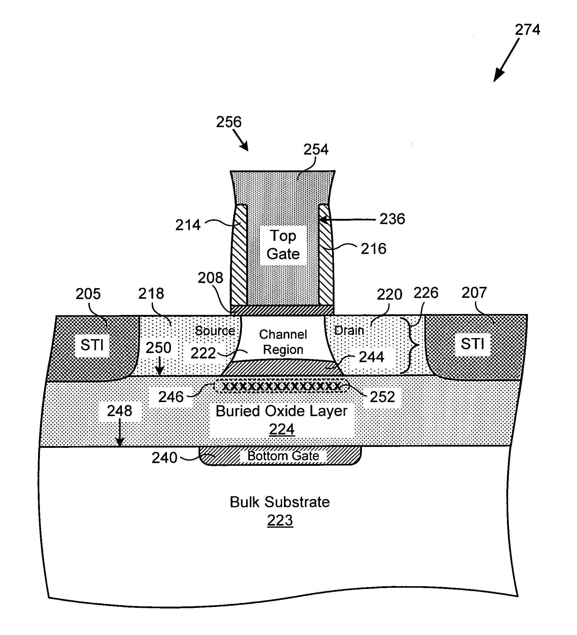
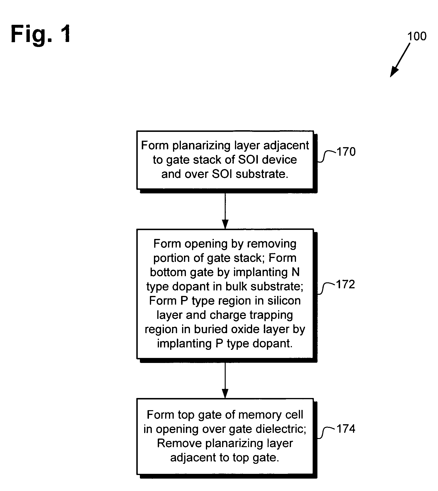
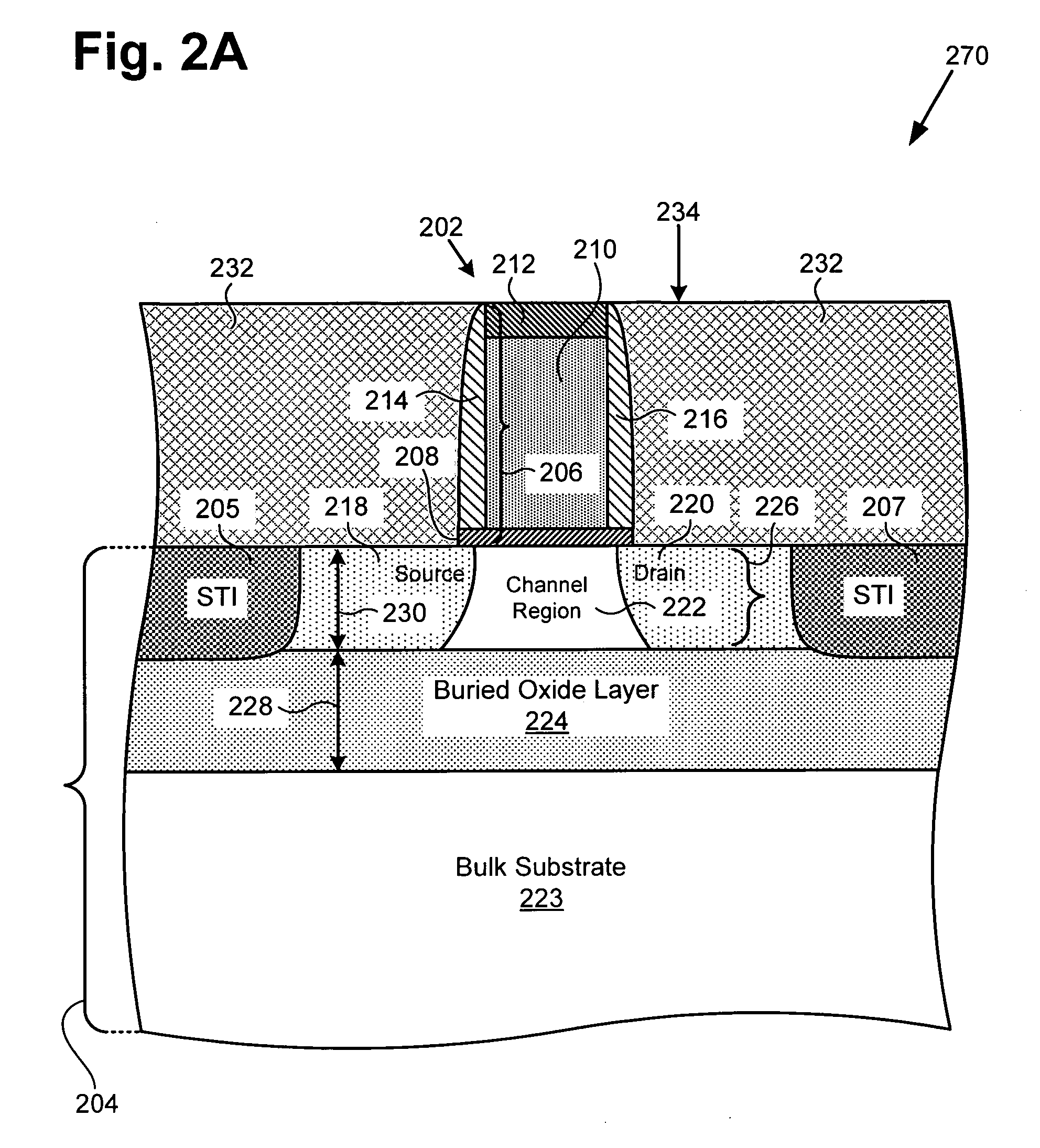
[0012]The present invention is directed to method for forming a one transistor memory cell and related structure. The following description contains specific information pertaining to the implementation of the present invention. One skilled in the art will recognize that the present invention may be implemented in a manner different from that specifically discussed in the present application. Moreover, some of the specific details of the invention are not discussed in order not to obscure the invention.

[0013]The drawings in the present application and their accompanying detailed description are directed to merely exemplary embodiments of the invention. To maintain brevity, other embodiments of the present invention are not specifically described in the present application and are not specifically illustrated by the present drawings. It should be borne in mind that, unless noted otherwise, like or corresponding elements among the figures may be indicated by like or corresponding refe...


PUM


Abstract

According to one exemplary embodiment, a method for fabricating a one-transistor memory cell includes forming an opening by removing a portion of a gate stack of a silicon-on-insulator (SOI) device, where the SOI device is situated over a buried oxide layer. The method further includes forming a bottom gate of the one-transistor memory cell in a bulk substrate underlying the buried oxide layer. The method further includes forming a charge trapping region in the buried oxide layer. The charge trapping region is formed at an interface between a silicon layer underlying the gate stack and the buried oxide layer. The charge trapping region causes the one-transistor memory cell to have an increased sensing margin. The method further includes forming a top gate of the one-transistor memory cell in the opening. Also disclosed is an exemplary one-transistor memory cell fabricated utilizing the exemplary disclosed method.

Description

TECHNICAL FIELD[0001]The present invention is generally in the field of semiconductor devices. More particularly, the invention is in the field of fabrication of memory cells.BACKGROUND ART[0002]Dynamic random access memory (DRAM) is a type of volatile memory that generally provides high density with sufficient speed. In the quest to achieve even higher density, a technique for one-transistor DRAM cells has been developed. The individual memory cell is provided on a semiconductor-on-insulator (SOI) substrate, requires only a single transistor, and does not require a capacitor, which has historically been used in DRAM cells. This type of DRAM cell is also known as a capacitorless DRAM cell since it does not require a capacitor.[0003]A one-transistor DRAM cell typically includes a top gate, which is situated over the body of the transistor, and a bottom gate, which is situated in a bulk substrate underlying a buried oxide layer in the SOI substrate. The one-transistor DRAM cell can be...

Claims


Application Information

Patent Timeline
Patent Type & Authority Patents(United States)
IPC IPC(8): H01L27/12
CPCG11C11/404H01L21/2652H01L27/108H01L27/10802H01L29/105H01L29/66545H01L29/7841H01L29/78603H01L29/78696G11C2211/4016H01L21/28114H10B12/20H10B12/00
Inventor KRIVOKAPIC, ZORAN
Owner GLOBALFOUNDRIES U S INC
Why Eureka
Try Eureka