Thin film transistor and method of fabricating the same

a technology of thin film transistors and thin films, applied in the direction of transistors, electrical devices, semiconductor devices, etc., can solve the problems of low operating speed and electron mobility, complex fabrication process, and easy contamination or d

Active Publication Date: 2006-02-16
SAMSUNG DISPLAY CO LTD
View PDF4 Cites 70 Cited by
  • Summary
  • Abstract
  • Description
  • Claims
  • Application Information

AI Technical Summary

Benefits of technology

[0019] The present invention, therefore, solves aforementioned problems associated with conventional devices by providing a bottom gate thin film transistor and method of fabricating the same having a channel region crystallized by an SGS crystallization method by forming a gate electrode and a gate insulating layer on an insulating substrate; forming an amorphous silicon l...

Problems solved by technology

However, the top-gate thin film transistor has a drawback in that the fabrication process is complicated.
Moreover, an interface between the gate insulating layer and the semiconductor layer is exposed so that it is susceptible to conta...

Method used


Image

  • Thin film transistor and method of fabricating the same
  • Thin film transistor and method of fabricating the same
  • Thin film transistor and method of fabricating the same

Examples


first embodiment

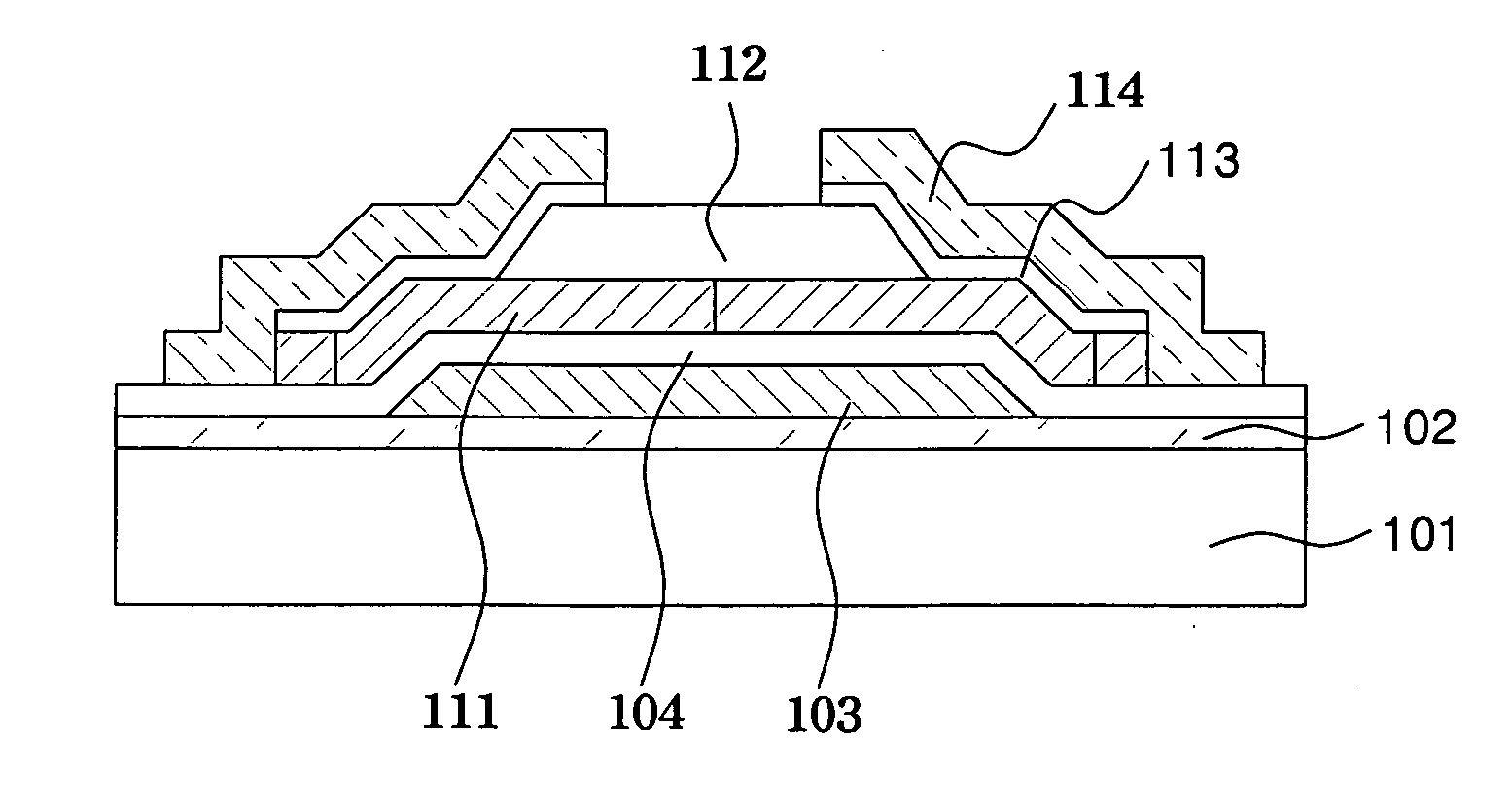
[0031]FIGS. 2A to 2D are cross-sectional views illustrating a process of fabricating a thin film transistor according to a first embodiment of the present invention.

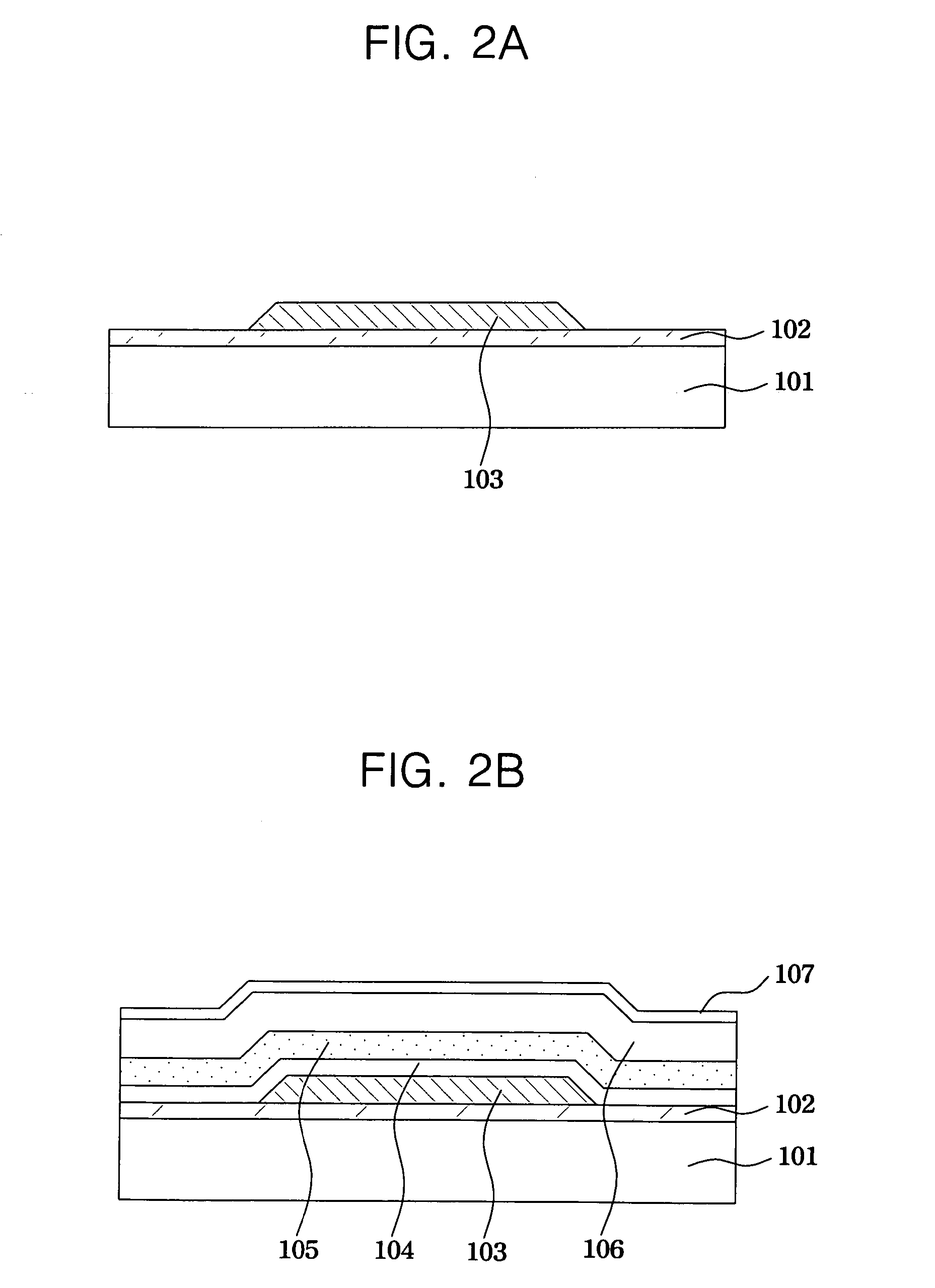
[0032]FIG. 2A is a cross-sectional view of a process of forming a buffer layer and a gate electrode on a substrate. As shown in FIG. 2A, a buffer layer 102 is formed on a transparent insulating substrate 101 such as glass or plastic, and a material for forming a gate electrode is formed on the buffer layer 102 and patterned to form a gate electrode 103. Here, the buffer layer 102 serves to prevent moisture or impurity generated from the lower substrate from diffusing.

[0033]FIG. 2B is a cross-sectional view of a process of sequentially forming a gate insulating layer, an amorphous silicon layer, a capping layer and a metal catalyst layer on the substrate on which the gate electrode is formed. As shown in FIG. 2B, a gate insulating layer 104 is formed on the substrate on which the gate electrode 103 is formed in a single...

second embodiment

[0047]FIGS. 3A to 3D are cross-sectional views illustrating a process of fabricating a thin film transistor according to a second embodiment of the present invention.

[0048]FIG. 3A is a cross-sectional view of a process of sequentially forming a buffer layer, a gate electrode, a gate insulating layer, an amorphous silicon layer, a capping layer and a metal catalyst layer on a substrate. As shown in FIG. 3A, a buffer layer 202 is formed on a transparent insulating substrate 201 such as glass or plastic, and a material for forming a gate electrode forming is deposited on the buffer layer 202 and patterned to form a gate electrode 203, in the same manner as that described in the first embodiment.

[0049] Next, a gate insulating layer 204 made of a silicon oxide layer or a silicon nitride layer in a single or double layer is formed on the substrate 201, and an amorphous silicon layer 205 is formed on the gate insulating layer 204.

[0050] Next, a capping layer 206 made of a silicon oxide ...

third embodiment

[0062]FIGS. 4A to 4C are cross-sectional views illustrating a process of fabricating a thin film transistor according to a third embodiment of the present invention.

[0063]FIG. 4A is a cross-sectional view of a process of sequentially forming a buffer layer, a gate electrode, a gate insulating layer, an amorphous silicon layer, a capping layer and a metal catalyst layer on a substrate. As shown in FIG. 4A, a buffer layer 302 is deposited on a transparent insulating substrate 301 such as glass or plastic, and a material for forming a gate electrode is deposited on the buffer layer 302 and patterned to form a gate electrode 303, in the same manner as that described in the first embodiment.

[0064] Next, a gate insulating layer 304 made in a single or double layer of a silicon oxide layer or a silicon nitride layer is formed on the substrate 301, and an amorphous silicon layer 305 is formed on the gate insulating layer 304.

[0065] Next, a capping layer 306 made of a silicon oxide layer ...


PUM


Abstract

A bottom gate thin film transistor and method of fabricating the same are disclosed, in which a channel region is crystallized by a super grain silicon (SGS) crystallization method, including: forming a gate electrode and a gate insulating layer on an insulating substrate; forming an amorphous silicon layer on the gate insulating layer followed by forming a capping layer and a metal catalyst layer; performing heat treatment to crystallize the amorphous silicon layer into a polysilicon layer; and forming an etch stopper, source and drain regions and source and drain electrodes. The thin film transistor includes: an insulating substrate; a gate electrode formed on the substrate; a gate insulating layer formed on the gate electrode; a polysilicon layer formed on the gate insulating layer and crystallized by an SGS crystallization method; and source and drain regions and source and drain electrodes formed in a predetermined region of the substrate. As described, a method of fabricating the conventional top-gate thin film transistor has problems in that an interface between a channel region and a gate insulating layer is directly exposed to air or in direct contact with a photoresist pattern or etchant so that the thin film transistor may be contaminated by impurities such as oxide, organic and metal, or damaged in grains, and in that a metal catalyst remains at an interface in crystallization so that leakage current may occur. However, advantageously, a method of fabricating a bottom-gate thin film transistor according to the present invention has merits in that an interface between the channel region and the gate insulating layer is not exposed to air so that the aforementioned problems do not occur. Therefore, a thin film transistor having excellent characteristics may be fabricated and a fabrication process thereof may be simplified.

Description

CROSS-REFERENCE TO RELATED APPLICATION [0001] This application claims the benefit of Korean Patent Application No. 2004-64033, filed Aug. 13, 2004, the disclosure of which is hereby incorporated herein by reference in its entirety. BACKGROUND OF THE INVENTION [0002] 1. Field of the Invention [0003] The present invention relates to a thin film transistor and method of fabricating the same and, more specifically, to a bottom gate thin film transistor and method of fabricating the same having a channel region crystallized by a super grain silicon (SGS) crystallization method by forming a gate electrode and a gate insulating layer on an insulating substrate, forming an amorphous silicon layer on the gate insulating layer followed by forming a capping layer and a metal catalyst layer, performing heat treatment to crystallize the amorphous silicon layer into a polysilicon layer, and forming an etch stopper, source and drain regions and source and drain electrodes. [0004] 2. Description of...

Claims


Application Information

Patent Timeline
IPC IPC(8): H01L29/786H01L21/84
CPCH01L21/2022H01L29/04H01L29/78696H01L29/78609H01L29/78678H01L29/66765H01L21/02491H01L21/02422H01L21/02488H01L21/02532H01L21/02496H01L21/02675H01L21/02505H01L21/02672
Inventor SEO, JIN-WOOKLEE, KI-YONGYANG, TAE-HOONPARK, BYOUNG-KEON
Owner SAMSUNG DISPLAY CO LTD
Why Eureka
Try Eureka