Method of Growing Uniform Semiconductor Nanowires without Foreign Metal Catalyst and Devices Thereof

a technology of semiconductor nanowires and metal catalysts, applied in the field of semiconductor nanowires, can solve the problems of low affecting the health and safety of mercury content, and requiring long tubes and limiting power output, and reducing the efficiency of such light sources

Active Publication Date: 2011-06-02
MCGILL UNIV
View PDF14 Cites 87 Cited by
  • Summary
  • Abstract
  • Description
  • Claims
  • Application Information

AI Technical Summary

Problems solved by technology

However, the efficiency of such light sources is woefully low.
However, whilst CFLs provide an immediate and visible statement by Governments and other organizations worldwide that they are addressing global climate change, environmental issues etc they are not a panacea.
Amongst the disadvantages of fluorescent lights are frequent switching limiting lifetime, health and safety from the mercury content, UV emissions which affect some materials, flicker affecting individuals with autism, epilepsy, lupus, chronic fatigue syndrome, and vertigo, radio interference, operating temperature where efficiency drops with increasing/decreasing temperature from room temperature, non-operation at below freezing, low-luminance requiring long tubes and limiting power output, dimming, and recycling through the phosphor and mercury.
As such the majority of the lighting market remains inaccessible despite the considerable research effort and investment have been expended.
This arises due to the challenges in realizing suitable LED technologies and devices using conventional quantum well structures, these including the relatively low internal quantum efficiency of these structures, the low light extraction efficiency realized, and relatively high device fabrication costs.
The extremely large inhomogeneous broadening observed makes it difficult to study the fundamental properties of InN, including the temperature dependence of the band gap and the electron concentration.
Additionally, the poorly defined wire geometry leads to uncontrolled electrical and optical properties, severely limiting their device applications.
Further the direct growth of InN on silicon, the most suitable substrate for InN in terms of lattice and thermal mismatches, has been further complicated by the development of an amorphous SiNx layer during the initial stage of growth, see J. Grandal et al.
Attempts to adjust these growth techniques, either by t

Method used


Image

  • Method of Growing Uniform Semiconductor Nanowires without Foreign Metal Catalyst and Devices Thereof
  • Method of Growing Uniform Semiconductor Nanowires without Foreign Metal Catalyst and Devices Thereof
  • Method of Growing Uniform Semiconductor Nanowires without Foreign Metal Catalyst and Devices Thereof

Examples


Embodiment Construction

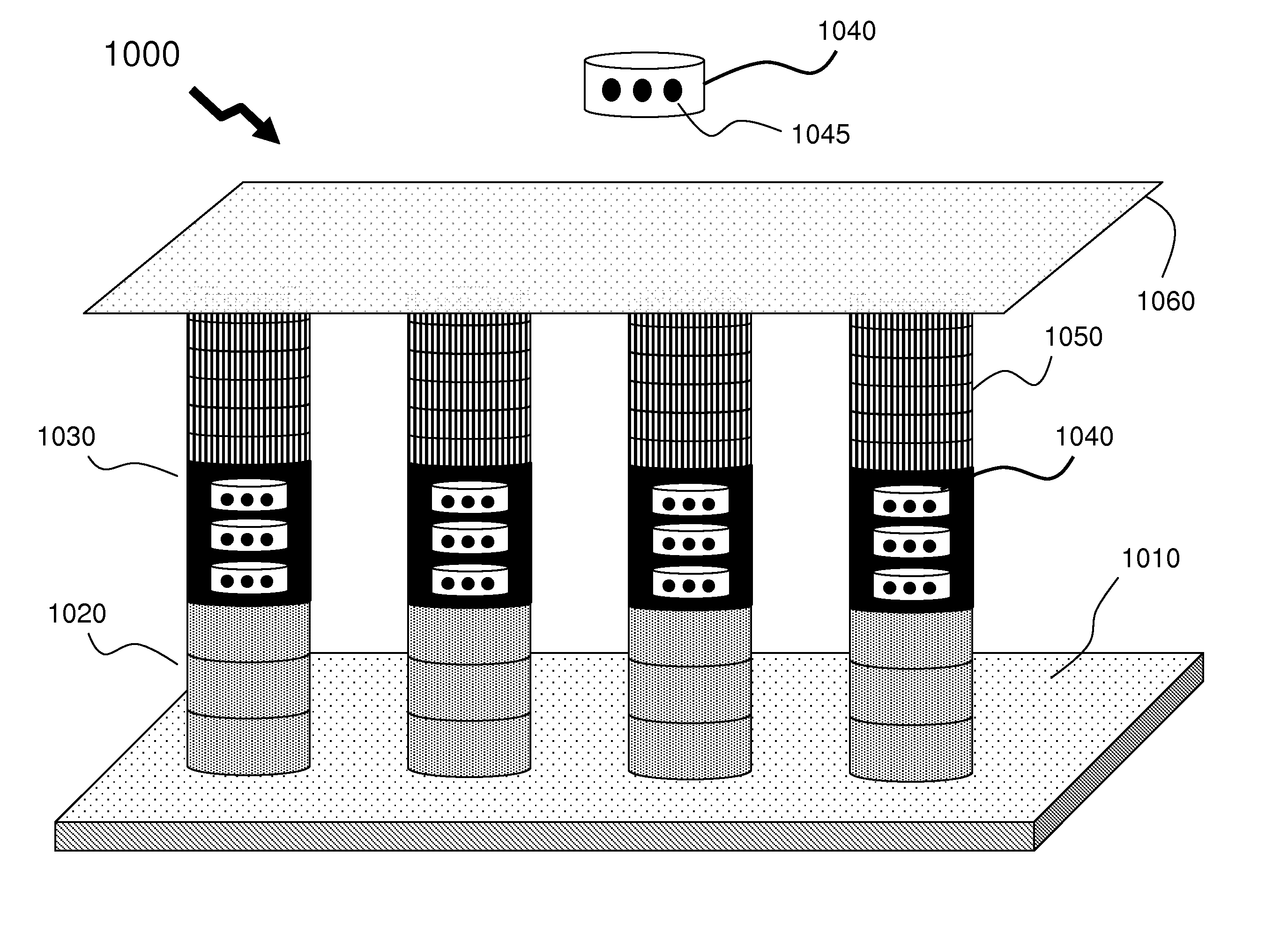
[0067]The present invention is directed to the growth of InGaN nanowires and devices thereof for high efficiency solid state light sources.

[0068]Reference may be made below to specific elements, numbered in accordance with the attached figures. The discussion below should be taken to be exemplary in nature, and not as limiting of the scope of the present invention. The scope of the present invention is defined in the claims, and should not be considered as limited by the implementation details described below, which as one skilled in the art will appreciate, can be modified by replacing elements with equivalent functional elements.

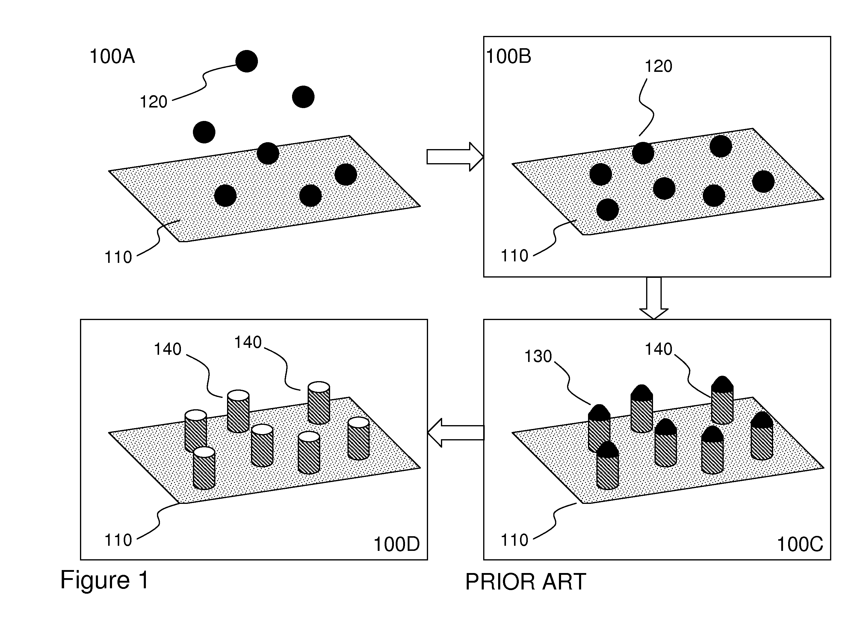
[0069]Referring to FIG. 1 there is shown a sequence of growing nanowires according to the prior art with a foreign metal catalyst. Such prior art using the vapor-liquid-solid (VLS) growth mechanism including for example J. Li et al in U.S. Pat. No. 6,831,017 entitled “Catalyst Patterning for Nanowire Devices”, L. Romano et al in U.S. Pat. No. 7,344,961 ent...


PUM


Abstract

Amongst the candidates for very high efficiency solid state lights sources and full solar spectrum solar cells are devices based upon InGaN nanowires. Additionally these nanowires typically require heterostructures, quantum dots, etc which all place requirements for these structures to be grown with relatively few defects. Further manufacturing requirements demand reproducible nanowire diameter, length etc to allow these nanowires to be embedded within device structures. Additionally flexibility according to the device design requires that the nanowire at the substrate may be either InN or GaN. According to the invention a method of growing relatively defect free nanowires and associated structures for group III—nitrides is presented without the requirement for foreign metal catalysts and overcoming the non-uniform growth of prior art non-catalyst growth techniques. The technique also allows for unique dot-within-a-dot nanowire structures.

Description

CROSS-REFERENCE TO RELATED APPLICATIONS[0001]This patent application claims the benefit of U.S. Provisional Patent Application 61 / 264,905 filed Nov. 30, 2009 entitled “Method of Growing Uniform Semiconductor Nanowires without Foreign Metal Catalyst and Devices Thereof.”FIELD OF THE INVENTION[0002]This invention relates to semiconductor nanowires and more specifically to a method of growth without a foreign metal catalyst and devices incorporating them thereof.BACKGROUND OF THE INVENTION[0003]The ability to generate and manipulate light with electricity by Sir Humphrey Davy 200 years ago sparked a century of development by the likes of Thomas Edison, Joseph Swan, Sandor Just (tungsten filaments), and Irving Langmuir (inert gas instead of vacuum) leading to the establishment 100 years ago of tungsten filament lamps, which as the dominant light source have fundamentally shifted how people live, work, play. However, the efficiency of such light sources is woefully low. For example a 60 ...

Claims


Application Information

Patent Timeline
IPC IPC(8): H01L29/66H01L21/20H01L33/06
CPCB82Y10/00Y02E10/548H01L21/02603H01L21/0262H01L21/02645H01L29/0676H01L31/035227H01L31/035281H01L31/075H01L31/184H01L31/1848H01L33/007H01L33/08H01L33/18Y02E10/544H01L21/0254
Inventor MI, ZETIAN
Owner MCGILL UNIV
Why Eureka
Try Eureka