Thin film transistors using thin film semiconductor materials

a technology of thin film semiconductor materials and transistors, which is applied in the direction of transistors, semiconductor devices, electrical appliances, etc., can solve the problems of low mobility of silicon, high temperature of amorphous silicon, and vth shi

Active Publication Date: 2009-02-26
APPLIED MATERIALS INC
View PDF99 Cites 63 Cited by
  • Summary
  • Abstract
  • Description
  • Claims
  • Application Information

AI Technical Summary

Benefits of technology

[0009]The present invention generally comprises TFTs having semiconductor material comprising oxygen, nitrogen, and one or more element selected from the group consisting of zinc, tin, gallium, cadmium, and indium as the active channel. The semiconductor material may be used in bottom gate TFTs, top gate TFTs, and other types of TFTs. The TFTs may be patterned by etching to create both the channel and the metal electrodes. Then, the source-drain electrodes may be defined by dry etching using the semiconductor material as an etch stop layer. The active layer carrier concentration, mobility, and interface with other layers of the TFT can be tuned to predetermined values. The tuning may be accomplished by changing the nitrogen containing gas to oxygen containing gas flow ratio, annealing and / or plasma treating the deposited semiconductor film, or changing the concentration of aluminum doping.
[0010]In one embodiment, a TFT is disclosed. The transistor comprises a semiconductor layer comprising oxygen, nitrogen and one or more elements selected from the group consisting of zinc, indium, tin, cadmium, gallium, and combinations thereof. In another embodiment, a TFT fabrication method is disclosed. The method comprises depositing a semiconductor layer over a substrate, the semiconductor layer comprising oxygen, nitrogen and one or more elements selected from the group consisting of zinc, indium, tin, cadmium, gallium, and combinations thereof.
[0011]In another embodiment, a TFT fabrication method is disclosed. The method comprises depositing a semiconductor layer over a substrate, the semiconductor layer comprising oxygen, nitrogen and one or more elements selected from the group consisting of an element having filled s and d orbitals, an element having a filled f orbital, and combinations thereof. The method also includes depositing a source-drain electrode layer over the active channel layer, first etching the source-drain electrode layer and the active channel layer to create an active channel, and second etching the source-drain electrode layer to define source-drain electrodes.

Problems solved by technology

Unfortunately amorphous silicon does have its limitations such as low mobility.
The deposition temperature for amorphous silicon may be high, which can cause a Vth shift.
A high current may be necessary for amorphous silicon, which can lead to stability issues in OLEDs.
Polysilicon is crystalline, which leads to non-uniform deposition.
Due to the limitations of amorphous silicon, OLED advancement has been difficult.
Zinc oxide, while having a mobility greater than amorphous silicon, still has a low mobility.

Method used


Image

  • Thin film transistors using thin film semiconductor materials
  • Thin film transistors using thin film semiconductor materials
  • Thin film transistors using thin film semiconductor materials

Examples


Embodiment Construction

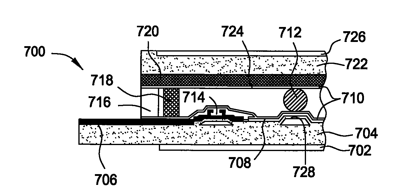
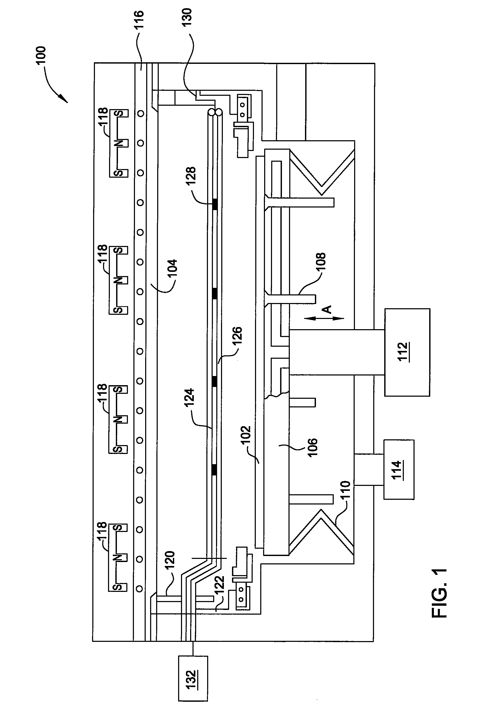
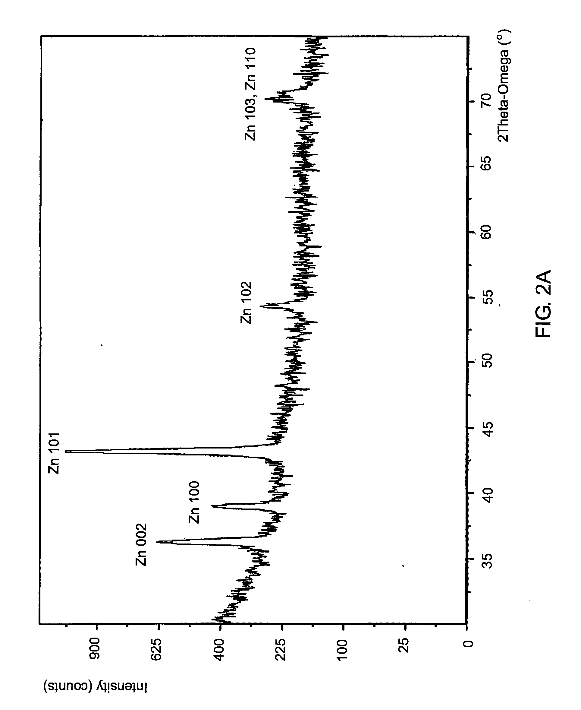
[0024]The present invention generally comprises TFTs having semiconductor material comprising oxygen, nitrogen, and one or more element selected from the group consisting of zinc, tin, gallium, cadmium, and indium as the active channel. The semiconductor material may be used in bottom gate TFTs, top gate TFTs, and other types of TFTs. The TFTs may be patterned by etching to create both the channel and the metal electrodes. Then, the source-drain electrodes may be defined by dry etching using the semiconductor material as an etch stop layer. The active layer carrier concentration, mobility, and interface with other layers of the TFT can be tuned to predetermined values. The tuning may be accomplished by changing the nitrogen containing gas to oxygen containing gas flow ratio, annealing and / or plasma treating the deposited semiconductor film, or changing the concentration of aluminum doping.

[0025]The semiconductor film comprising nitrogen, oxygen, and one or more elements selected fro...


PUM


Abstract

The present invention generally comprises TFTs having semiconductor material comprising oxygen, nitrogen, and one or more element selected from the group consisting of zinc, tin, gallium, cadmium, and indium as the active channel. The semiconductor material may be used in bottom gate TFTs, top gate TFTs, and other types of TFTs. The TFTs may be patterned by etching to create both the channel and the metal electrodes. Then, the source-drain electrodes may be defined by dry etching using the semiconductor material as an etch stop layer. The active layer carrier concentration, mobility, and interface with other layers of the TFT can be tuned to predetermined values. The tuning may be accomplished by changing the nitrogen containing gas to oxygen containing gas flow ratio, annealing and/or plasma treating the deposited semiconductor film, or changing the concentration of aluminum doping.

Description

CROSS-REFERENCE TO RELATED APPLICATIONS[0001]This application claims benefit of U.S. provisional patent application Ser. No. 60 / 953,683 (APPM / 012581L), filed Aug. 2, 2007, which is herein incorporated by reference.BACKGROUND OF THE INVENTION[0002]1. Field of the Invention[0003]Embodiments of the present invention generally relate to field effect transistors (FETs) and thin film transistors (TFTs) having semiconductor materials comprising oxygen, nitrogen, and one or more elements selected from the group consisting of zinc, gallium, cadmium, indium, and tin.[0004]2. Description of the Related Art[0005]Current interest in TFT arrays is particularly high because these devices may be used in liquid crystal active matrix displays (LCDs) of the kind often employed for computer and television flat panels. The LCDs may also contain light emitting diodes (LEDs) for back lighting. Further, organic light emitting diodes (OLEDs) have been used for active matrix displays, and these OLEDs require...

Claims


Application Information

Patent Timeline
Patent Type & Authority Applications(United States)
IPC IPC(8): H01L29/786H01L21/336
CPCH01L29/7869H01L27/1225H01L29/66742
Inventor YE, YAN
Owner APPLIED MATERIALS INC
Why Eureka
Try Eureka