

Materials for multicolor light emitting diodes
a light-emitting diode, multi-color technology, applied in the direction of application, discharge tube luminescnet screen, natural mineral layered products, etc., can solve the problems of low contrast and resolution, no other type of technology offers comparable speed, versatility and potential for interactivity, and lcd's operate fairly reliably, etc., to facilitate charge or excitation
- Summary
- Abstract
- Description
- Claims
- Application Information
AI Technical Summary
Problems solved by technology
Method used
Image

Examples
example 1
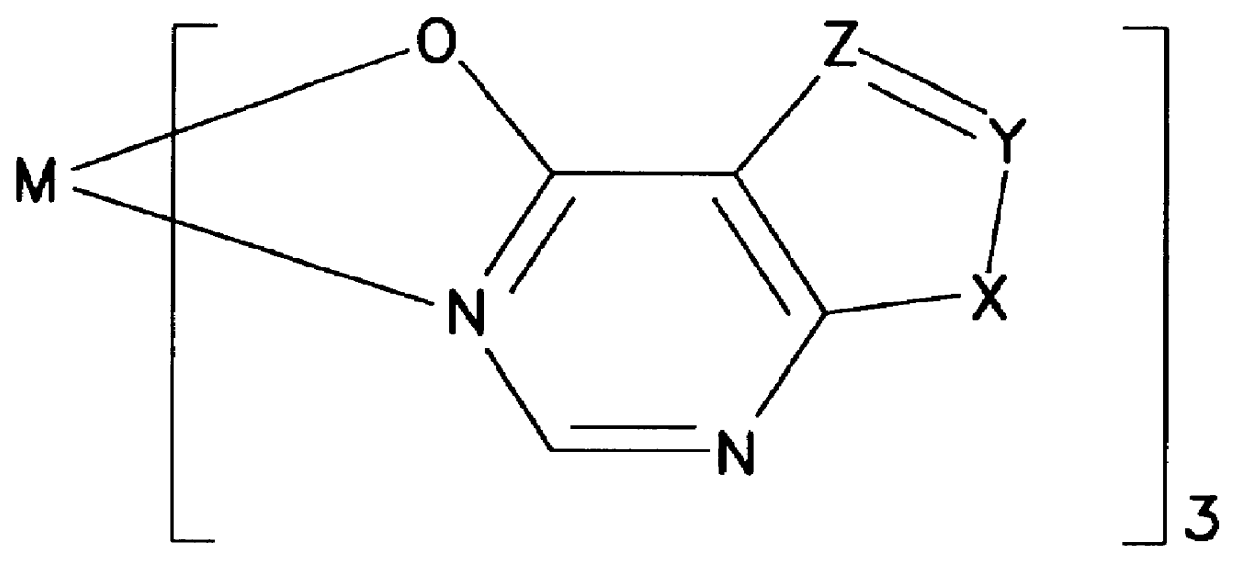
Preparation of Compounds of Formula I
A 0.25-g sample of 4-hydroxypyrazolo[3,4-d]pyrimidine is dissolved in 2.5 mL of aqueous 1.1 M NaOH. A solution prepared by dissolving 0.114 g of gallium nitrate in 1.5 mL of water is added slowly to the NaOH solution. A precipitate forms upon addition of the gallium nitrate. The white precipitate was isolated by filtration, washed twice with 5-mL aliquots of ethanol, and air dried. The isolated product, when excited at 250 nm, has an emission maximum at 390 nm.
example 2
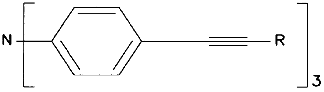
Preparation of Compounds of Formula II
A. Preparation of tris(4-ethylphenyl)amine [N(C.sub.6 H.sub.4 CCH).sub.3 ]
A solution of aqueous KOH is prepared by dissolving 1.26 g (0.0225 mol) in methanol. The KOH solution is added to a solution of tris(4-trimetylsilylethynylphenyl)amine that was prepared by adding 2.00 g (0.0038 mol) to 100 mL of tetrahydrofuran (THF), creating an orange solution that was stirred at room temperature for 3 hours. The small amount of orange precipitate that formed was removed by filtering the reaction mixture through Celite. The Celite was washed with two 10-mL portions of THF. The solvent was removed from the combined filtrates in vacuo leaving a gummy beige-orange residue. The residue was triturated with 50 mL of methanol and left to stir for one hour at room temperature. The product (corresponding to Formula II) was obtained as an orange powder that was collected, washed with 2 5-mL portions of pentane and dried in vacuo. Two additional crops were obtained...
example 3
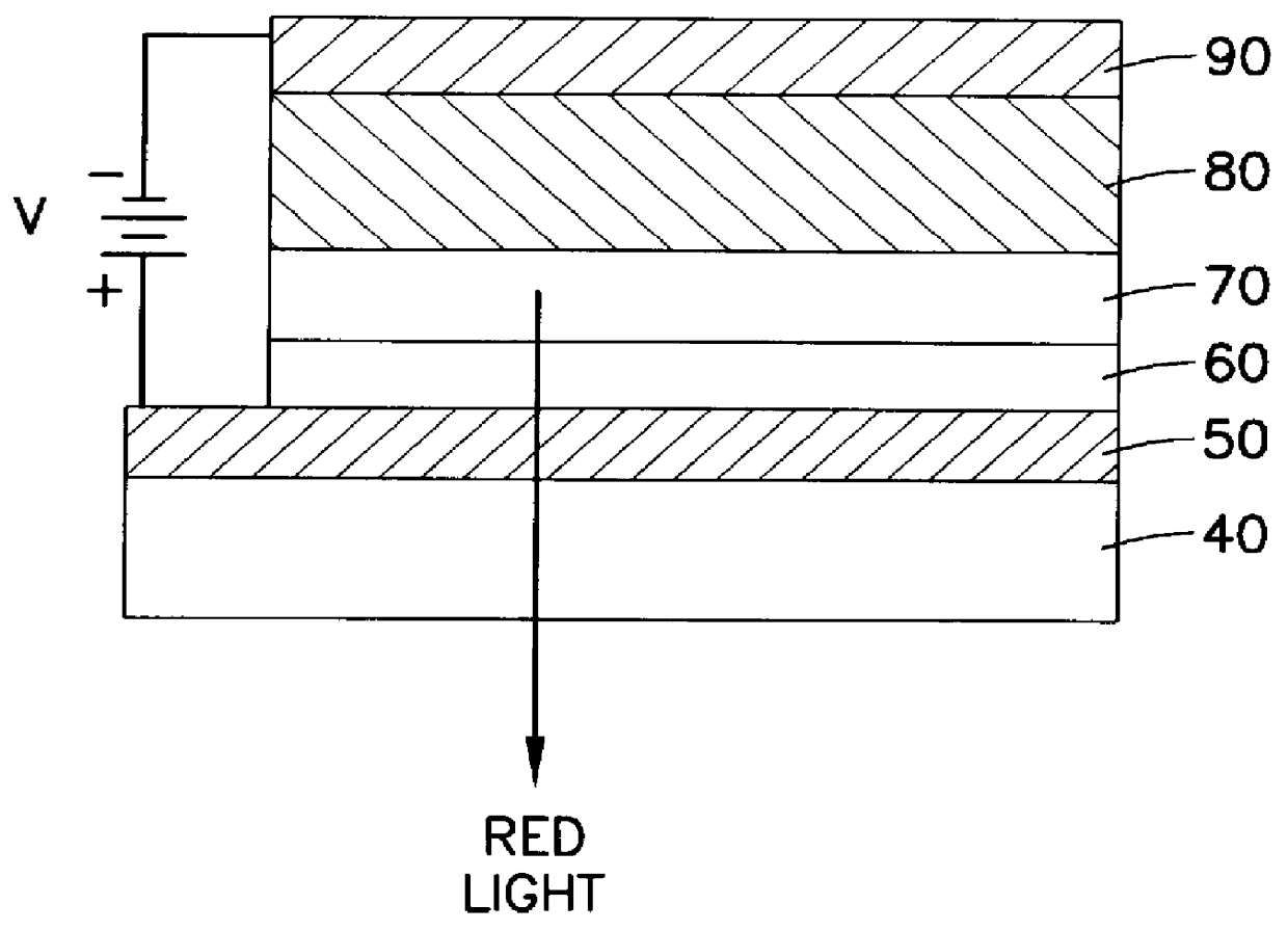
Preparation of an OLED According to the Present Invention
A. According to Formula I
A transparent substrate (e.g. glass or plastic) is precoated with an indium tin oxide (ITO) layer having a sheet resistance of about 15 ohm / square. The substrate may be cleaned by thorough rinsing in deionized water, 1,1,1-trichloroethane, acetone and methanol, and dried in pure nitrogen gas between each step. The clean, dry substrate is then transferred to the vacuum deposition system. All organic and metal depositions may then be carried out under high vacuum (<2.times.10.sup.-6 torr). Depositions are carried out by thermal evaporation from baffled Ta crucibles at a nominal deposition rate of 2-4 angstroms / second. First, an approximately 350 angstrom layer of N,NI-diphenyl-N,N'-bis(3-methylphenyl)-1,11-biphenyl-4,41-diamine (TPD) may be vapor deposited onto the cleaned ITO substrate. A sample of a compound according to Formula I and a selected fluorescent dye are then heated in separate Ta boats to d...
PUM
| Property | Measurement | Unit |
|---|---|---|
| transparency | aaaaa | aaaaa |
| transparency | aaaaa | aaaaa |
| thick | aaaaa | aaaaa |
Abstract
Description
Claims
Application Information