MOCVD GROWTH TECHNIQUE FOR PLANAR SEMIPOLAR (Al, In, Ga, B)N BASED LIGHT EMITTING DIODES

Inactive Publication Date: 2009-12-17
RGT UNIV OF CALIFORNIA
View PDF20 Cites 159 Cited by
  • Summary
  • Abstract
  • Description
  • Claims
  • Application Information

AI Technical Summary

Benefits of technology

[0018]The LED or laser diode may have a semipolar orientation, for example. If the quantum well layer is semipolar (or nonpolar), then an amount of piezoelectric and spontaneous polarization of the well layer may be reduced as compared to a piezoelectric and spontaneous polarization of a c-plane indium containing quantum well layer. Alternatively, the indium containing quantum well layer's piezoelectric and sponta

Problems solved by technology
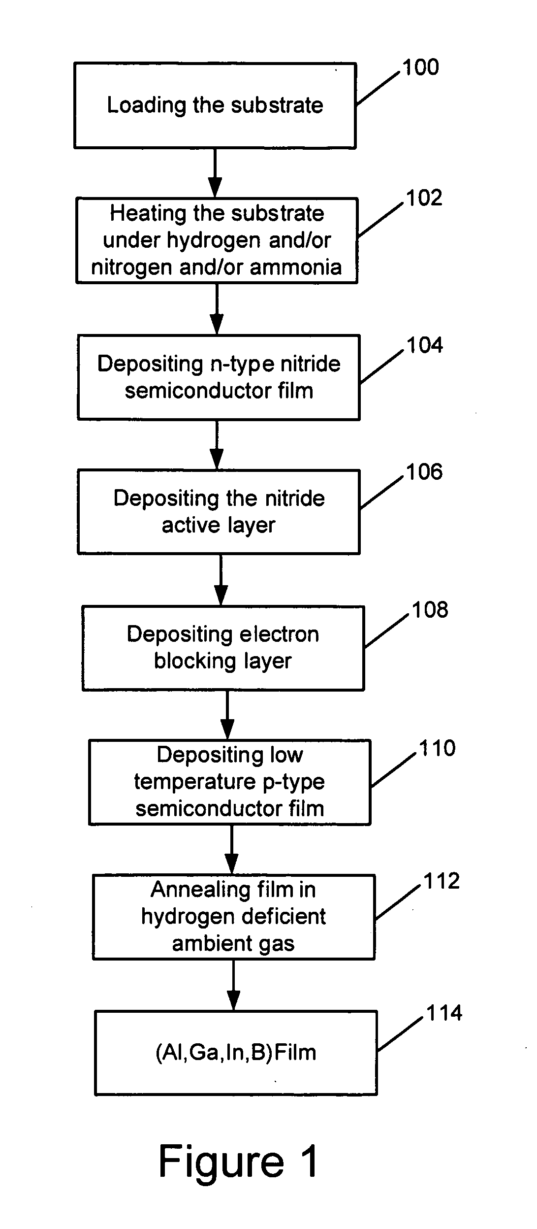
However, conventional c-plane quantum well structures in III-nitride based optoelectronic and electronic devices suffer from the undesirable quantum-confined Stark effect (QCSE), due to the existence of strong piezoelectric and spontaneous polarizations.
The strong built-in electric fields along the c-direction cause spatial separation of electrons and holes that in turn give rise to restrict

Method used


Image

  • MOCVD GROWTH TECHNIQUE FOR PLANAR SEMIPOLAR (Al, In, Ga, B)N BASED LIGHT EMITTING DIODES
  • MOCVD GROWTH TECHNIQUE FOR PLANAR SEMIPOLAR (Al, In, Ga, B)N BASED LIGHT EMITTING DIODES
  • MOCVD GROWTH TECHNIQUE FOR PLANAR SEMIPOLAR (Al, In, Ga, B)N BASED LIGHT EMITTING DIODES

Examples


Embodiment Construction

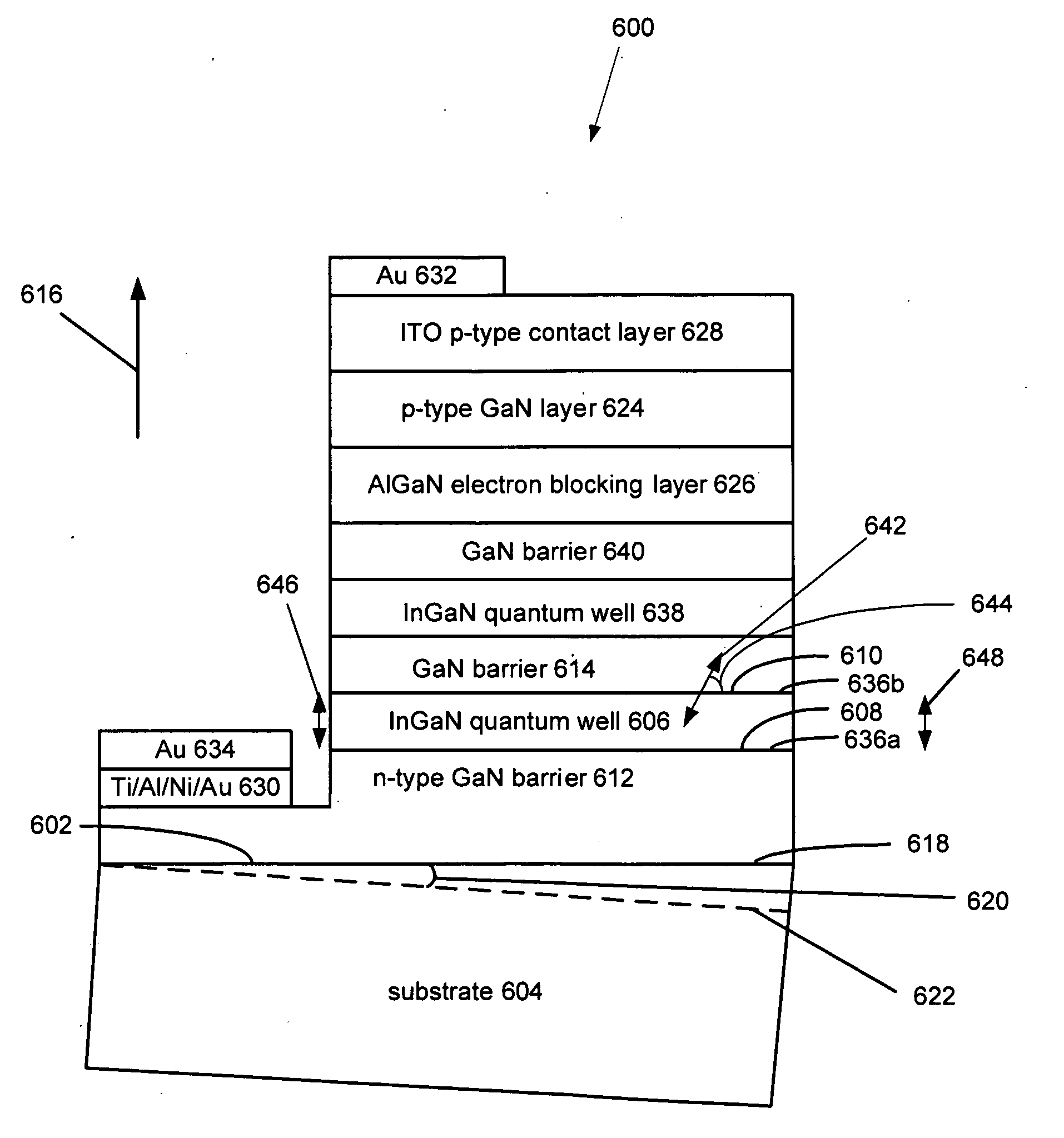
[0034]In the following description of the preferred embodiment, reference is made to the accompanying drawings which form a part hereof, and in which is shown by way of illustration a specific embodiment in which the invention may be practiced. It is to be understood that other embodiments may be utilized and structural changes may be made without departing from the scope of the present invention.

[0035]Overview

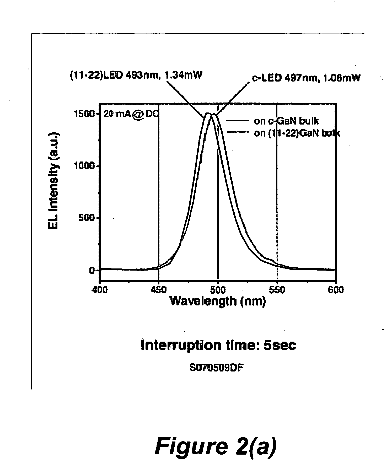
[0036]The present invention allows the growth of planar LEDs with longer wavelength emission (500 nm or higher) by incorporating more Indium in the well layer (InxGa1-xN) of a MQW or SQW, using MOCVD or MBE growth techniques. This will be an important method for fabricating and commercializing high power and high efficient nitride LEDs, especially in the range of wavelength from 560 nm to 680 nm, and nitride-based white LEDs.

[0037]Current AlInGaP-based yellow and amber LEDs are not suitable for high temperature and high injection current operations due to carrier overflow due ...


PUM


Abstract

A III-nitride optoelectronic device comprising a light emitting diode (LED) or laser diode with a peak emission wavelength longer than 500 nm. The III-nitride device has a dislocation density, originating from interfaces between an indium containing well layer and barrier layers, less than 9×109 cm−2. The III-nitride device is grown with an interruption time, between growth of the well layer and barrier layers, of more than 1 minute.

Description

CROSS REFERENCE TO RELATED APPLICATIONS[0001]This application claims the benefit under 35 U.S.C. Section 119(e) of co-pending and commonly-assigned U.S. Provisional Patent Application Ser. No. 61 / 042,639, filed on Apr. 4, 2008, by Hitoshi Sato, Roy B. Chung, Feng Wu, James S. Speck, Steven P. DenBaars and Shuji Nakamura, entitled “MOCVD GROWTH TECHNIQUE FOR PLANAR SEMIPOLAR (Al, In, Ga, B)N BASED LIGHT EMITTING DIODES,” attorney's docket number 30794.274-US-P1 (2008-534), which application is incorporated by reference herein.[0002]This application is related to co-pending and commonly-assigned U.S. Utility patent application Ser. No. ______, filed on same date herewith, by Hitoshi Sato, Hirohiko Hirasawa, Roy B. Chung, Steven P. DenBaars, James S. Speck and Shuji Nakamura, entitled “METHOD FOR FABRICATION OF SEMIPOLAR (Al,In,Ga,B)N BASED LIGHT EMITTING DIODES,” attorneys' docket number 30794.264-US-P1 (2008-415-1), which which application claims the benefit under 35 U.S.C. Section 1...

Claims


Application Information

Patent Timeline
IPC IPC(8): H01S5/343H01L29/66H01L33/00H01L21/20H01L33/06H01L33/16H01L33/32
CPCH01L21/02389H01L21/02433H01L21/0254H01L33/32H01L21/0262H01L33/06H01L33/16H01L21/02543
Inventor SATO, HITOSHICHUNG, ROY B.WU, FENGSPECK, JAMES S.DENBAARS, STEVEN P.NAKAMURA, SHUJI
Owner RGT UNIV OF CALIFORNIA
Why Eureka
Try Eureka