Liquid crystal display device and method of manufacturing the same

a liquid crystal display and liquid crystal technology, applied in the direction of identification means, instruments, optics, etc., can solve the problems of color tone change and unclearness

Inactive Publication Date: 2010-02-02
SEMICON ENERGY LAB CO LTD
View PDF323 Cites 63 Cited by
  • Summary
  • Abstract
  • Description
  • Claims
  • Application Information

AI Technical Summary

Benefits of technology

[0073]With the present invention, an electro-optical device of an IPS system prepared with a pixel TFT portion, having a reverse stagger type n-channel TFT, and a storage capacitor can be realized through three photolithography processes using three photomasks.
[0074]Further, when forming a protecting film, an electro-optical device of an IPS system prepared with a pixel TFT portion, having a reverse stagger type n-channel TFT protected by an inorganic insulating film, and a storage capacitor can be realized through four photolithography processes using four photomasks.

Problems solved by technology

However, such a driving method of a liquid crystal has a defect that an angle of view is narrow, that is, although a normal display state is obtained when it is viewed in a direction vertical to the substrate plane, a color tone is changed and becomes unclear when it is viewed in an oblique direction.

Method used


Image

  • Liquid crystal display device and method of manufacturing the same
  • Liquid crystal display device and method of manufacturing the same
  • Liquid crystal display device and method of manufacturing the same

Examples


embodiments

Embodiment 1

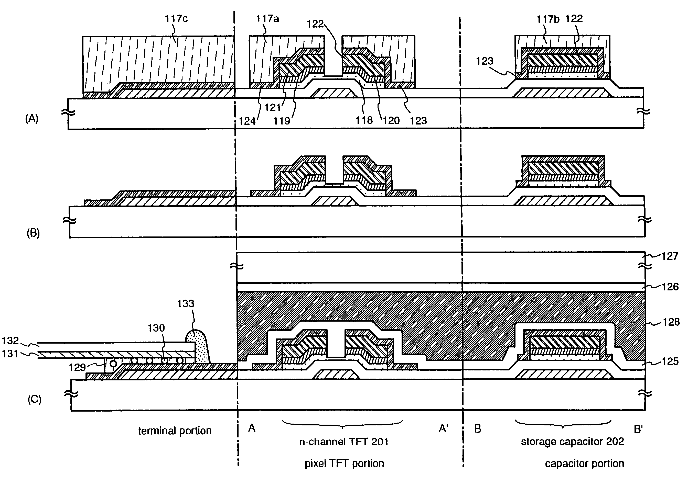
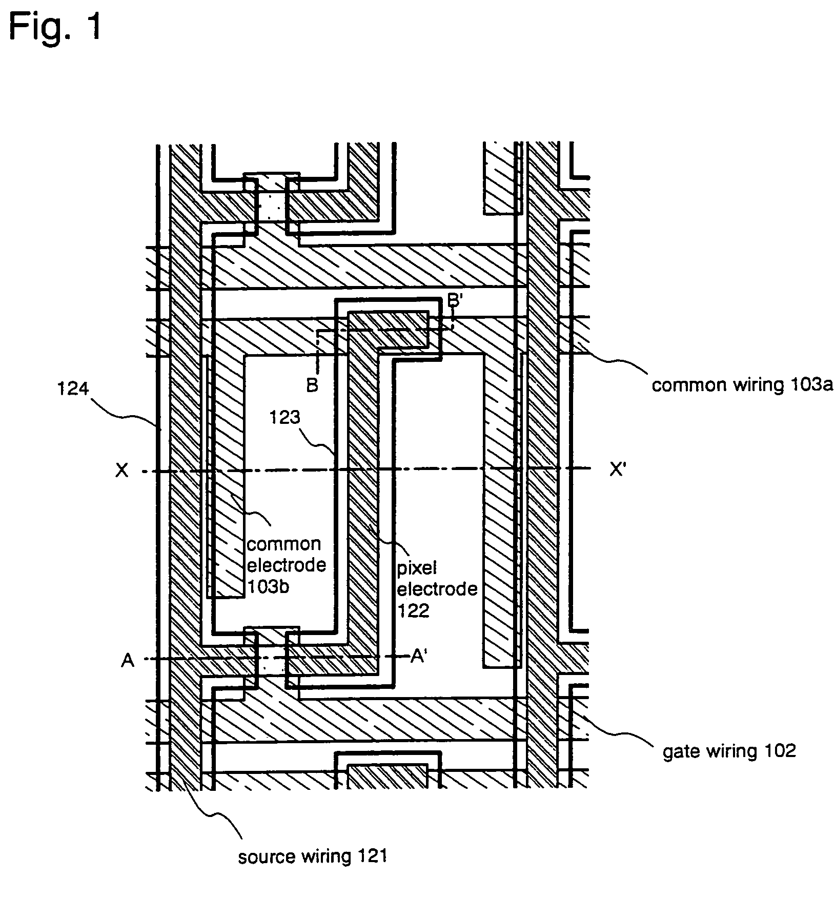
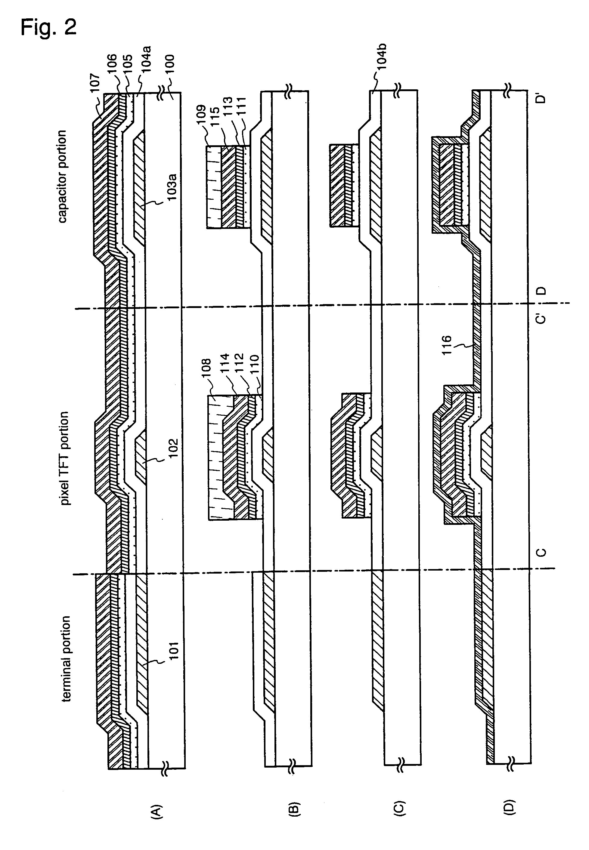
[0105]An embodiment of the invention is explained using FIGS. 1 to 7. This Embodiment shows a method of manufacturing a liquid crystal display device, and a detailed explanation of a method of forming a TFT of a pixel portion on a substrate by a reverse stagger type TFT (channel etching type), and manufacturing a storage capacitor connected to the TFT, is made in accordance with the processes used. Further, a manufacturing process for a terminal section, formed in an edge portion of the substrate, and for electrically connecting to wirings of circuits formed on other substrates, is shown at the same time in the same figures.

[0106]In FIG. 2(A), a glass substrate, comprising such as barium borosilicate glass or aluminum borosilicate glass, typically Corning Corp. #7059 glass or #1737 glass, can be used as a substrate 100 having translucency. In addition, a translucent substrate such as a quartz substrate or a plastic substrate can also be used.

[0107]Next, after forming a c...

embodiment 2

[0140]FIG. 8 is an example of a method of mounting a liquid crystal display device. The liquid crystal display device has an input terminal portion 302 formed in an edge portion of a substrate 301 on which TFTs are formed, and as shown by embodiment 1, this is formed by a terminal 303 formed from the same material as a gate wiring. An opposing substrate 304 is joined to the substrate 301 by a sealant 305 encapsulating spacers 306, and in addition, polarizing plates 307 and 308 and a color filter (not shown) are disposed. Note that the arrangement of one of the polarizing plate may be adjusted to the longer axis of the liquid crystal molecule and the arrangement of the other polarizing plate may be adjusted to the shorter axis of the liquid crystal molecule. This is then fixed to a casing 321 by spacers 322.

[0141]Note that the TFT obtained in Embodiment 1 having an active layer formed by an amorphous silicon film has a low electric field effect mobility, and only approximately 1 cm2 / ...

embodiment 3

[0143]In this Embodiment, an example of forming a protecting film is shown in FIG. 14. Note that this Embodiment is identical to Embodiment 1 through the state of FIG. 3(B), and therefore only points of difference are explained. Further, the same symbols are used for locations corresponding to those in FIG. 3(B).

[0144]After first forming through the state of FIG. 3(B) in accordance with Embodiment 1, a thin inorganic insulating film is formed on the entire surface. An inorganic insulating film formed by using plasma CVD or sputtering such as a silicon oxide film, a silicon nitride film, a silicon oxynitride film, or a tantalum oxide film is used as the thin inorganic insulating film, and a single layer or a lamination structure made from these materials may be formed.

[0145]A forth photolithography process is performed next, forming a resist mask, and unnecessary portions are removed by etching, forming an insulating film 402 in the pixel TFT portion, and an inorganic insulating film...


PUM

PropertyMeasurementUnit
viewing angleaaaaaaaaaa
pre-tilt angleaaaaaaaaaa
angleaaaaaaaaaa

Abstract

In a liquid crystal display device of an IPS system, to realize reduction of manufacturing cost and improvement of yield by decreasing the number of steps for manufacturing a TFT. A channel etch type bottom gate TFT structure, where patterning of a source region and a drain region and patterning of a source wiring and a pixel electrode are carried out by the same photomask.

Description

BACKGROUND OF THE INVENTION[0001]1. Field of the Invention[0002]The present invention relates to an active matrix type liquid crystal display device, and particularly to an active matrix type liquid crystal display device of an IPS (In-Plane Switching) system (=transverse electric field system).[0003]2. Description of Related Art[0004]An active matrix type liquid crystal display device using an active element such as a thin film transistor (TFT) is known. The active matrix type liquid crystal display device can increase pixel density, is small and lightweight, and consumes less power, so that as a substitute for a CRT, a product such as a monitor of a personal computer or a liquid crystal television has been developed. Especially, a technique of forming an active layer of a TFT by a crystalline semiconductor film typified by polycrystalline silicon makes it possible to form a driver circuit as well as a switching TFT for a pixel portion (hereinafter referred to as a pixel TFT) on th...

Claims


Application Information

Patent Timeline
Patent Type & Authority Patents(United States)
IPC IPC(8): G02F1/1343G02F1/1345G02F1/13G02F1/136G02F1/1362G02F1/1368G09F9/30H01L21/336H01L21/77H01L27/12H01L29/786
CPCG02F1/134363G02F1/13439G02F1/13458G02F1/1368H01L27/12H01L27/1214G02F1/136286G02F1/1396H01L27/124H01L29/78669G02F1/1337G02F1/133345H01L27/1222G02F1/133707G02F1/136277G02F1/136204G02F2001/136231G02F2001/13629G02F1/13452G02F1/136231E02B3/125E02D29/0208G02F1/13629
Inventor YAMAZAKI, SHUNPEIHIRAKATA, YOSHIHARU
Owner SEMICON ENERGY LAB CO LTD
Why Eureka
Try Eureka