

Atomic layer removal for high aspect ratio gapfill
a technology of high aspect ratio and gapfilling, which is applied in the direction of basic electric elements, semiconductor/solid-state device manufacturing, electric apparatus, etc., can solve the problems of reducing budgets, increasing the difficulty of void-free filling of narrow width, and increasing the difficulty of high aspect ratio (ar) features (e.g. ar>6:1)
Active Publication Date: 2011-07-19
NOVELLUS SYSTEMS
View PDF69 Cites 77 Cited by
- Summary
- Abstract
- Description
- Claims
- Application Information
AI Technical Summary
Benefits of technology
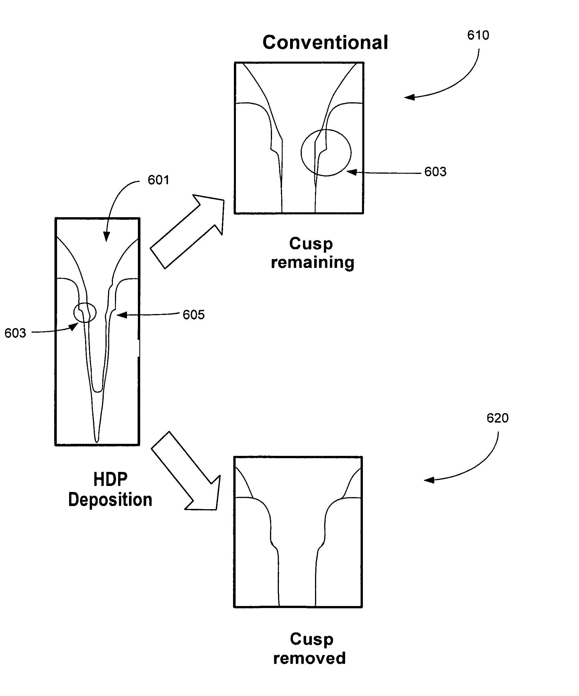
[0009]The present invention pertains to methods of filling high aspect ratio (typically at least 6:1, for example 7:1 or higher), narrow width (e.g., sub-50 nm) gaps on a substrate. The methods provide gap fill with little or no incidence of voids, seams or weak spots. According to various embodiments, the methods depositing dielectric material in the gaps to partially fill the gaps, then performing multi-step atomic layer removal process to selectively etch unwanted material deposited on the sidewalls of the gaps. The multi-step atomic layer removal process inv
Problems solved by technology
As device geometries shrink and thermal budgets are reduced, void-free filling of narrow width, high aspect ratio (AR) features (e.g., AR>6:1) becomes increasingly difficult due to limitations of existing deposition processes.
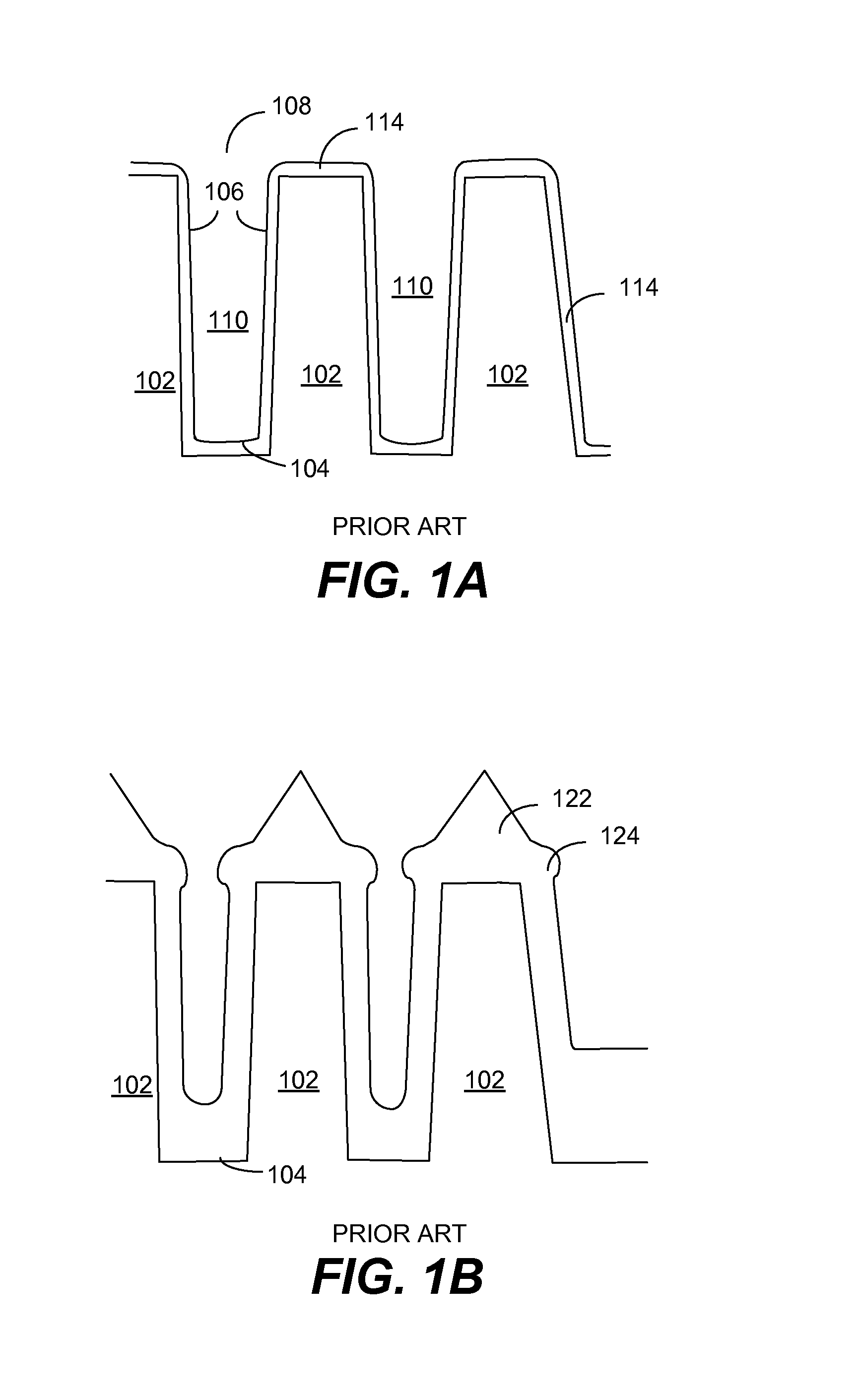
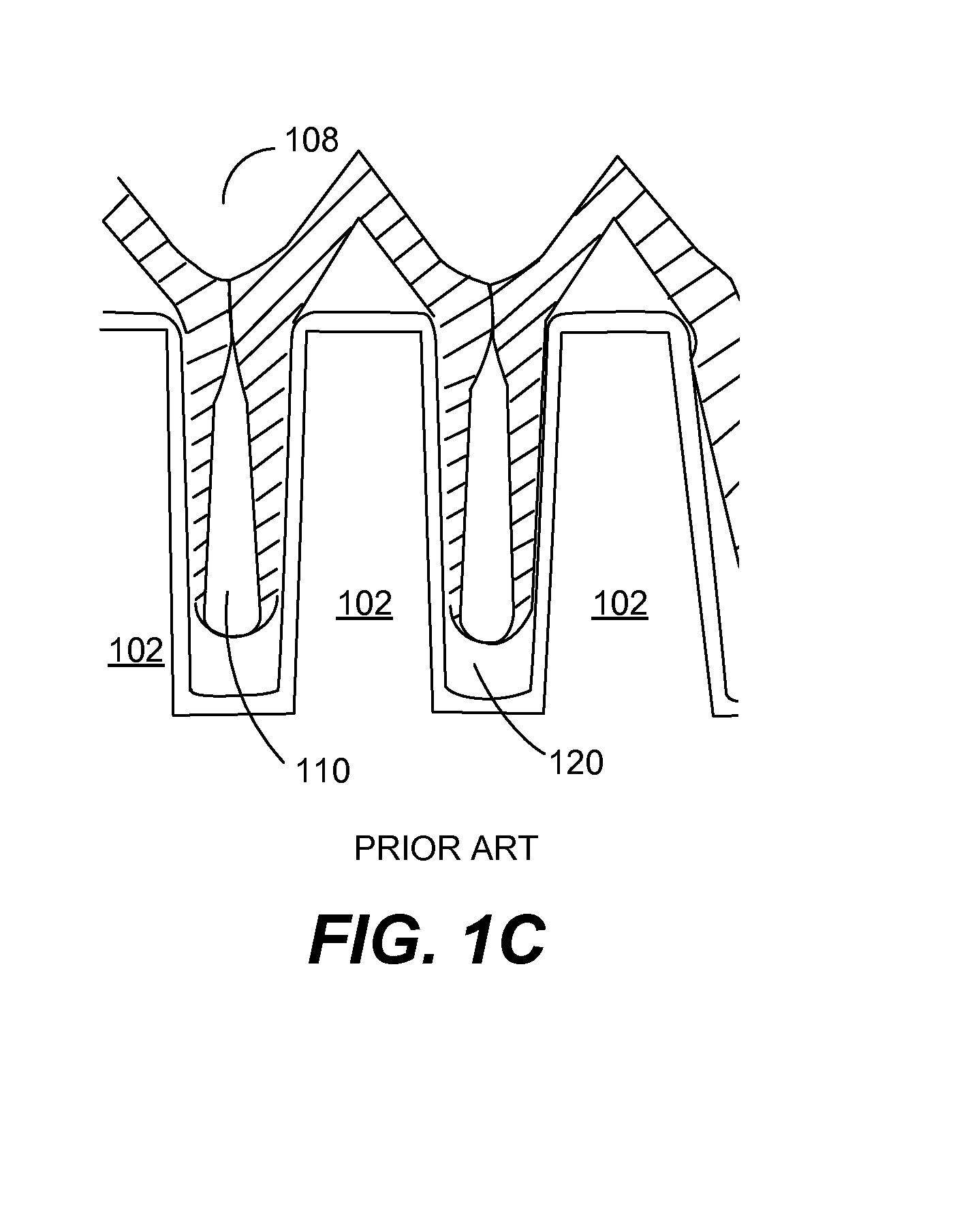
However, HDP CVD gapfill results in the formation of overhangs, at the entry region of the gap to be filled.
As a result, the entry region of a high aspect ratio structure may close bef
Method used
View moreImage
Smart ImageViewing Examples

Examples
 PUM
 Abstract
Methods of filling high aspect ratio, narrow width (e.g., sub-50 nm) gaps on a substrate are provided. The methods provide gap fill with little or no incidence of voids, seams or weak spots. According to various embodiments, the methods depositing dielectric material in the gaps to partially fill the gaps, then performing multi-step atomic layer removal process to selectively etch unwanted material deposited on the sidewalls of the gaps. The multi-step atomic layer removal process involves a performing one or more initial atomic layer removal operations to remove unwanted material deposited at the top of the gap, followed by one or more subsequent atomic layer removal operations to remove unwanted material deposited on the sidewalls of the gap. Each atomic layer removal operation involves selectively chemically reacting a portion of the fill material with one or more reactants to form a solid reaction product, which is then removed.
Description
CROSS REFERENCE TO RELATED APPLICATION[0001]This application claims priority under 35 U.S.C. §119(e) to U.S. Provisional Application 61 / 089,453 entitled “ATOMIC LAYER REMOVAL FOR HIGH ASPECT RATIO GAPFILL,” filed Aug. 15, 2008, all of which is incorporated in its entirety by this reference.FIELD OF THE INVENTION[0002]This invention relates to electronic device fabrication processes and associated apparatus. More specifically, the invention relates to deposition and dry etch processes for forming dielectric layers, particularly in filling gaps with high aspect ratios.BACKGROUND OF THE INVENTION[0003]It is often necessary in semiconductor processing to fill high aspect ratio gaps with insulating material. This is the case for shallow trench isolation (STI), inter-metal dielectric (IMD) layers, inter-layer dielectric (ILD) layers, pre-metal dielectric (PMD) layers, passivation layers, etc. As device geometries shrink and thermal budgets are reduced, void-free filling of narrow width, h...
Claims
Login to View More Application Information
Patent Timeline
 IPC IPC(8): H01L21/76
CPCH01L21/02274H01L21/31116H01L21/76837H01L21/76224
InventorVAN SCHRAVENDIJK, BARTTE NIJENHUIS, HARALD
OwnerNOVELLUS SYSTEMS