Brightness unevenness correction for OLED

a correction value and unevenness technology, applied in the field of brightness unevenness correction for oled, can solve the problems of manufacturing or aging deterioration, inability to determine an accurate correction value, etc., and achieve the effect of precise and efficient acquisition

Active Publication Date: 2011-07-19
GLOBAL OLED TECH
View PDF6 Cites 23 Cited by
  • Summary
  • Abstract
  • Description
  • Claims
  • Application Information

AI Technical Summary

Benefits of technology

[0029]With the present invention, correction data of brightness unevenness for an organic EL display can be precisely and efficiently acquired.

Problems solved by technology

This is caused by variation in the Vth of the TFT which drives the pixel and in the mobility (μ), which results from a problem in manufacturing or aging deterioration.
However, the error becomes large when Id is small, resulting in an inability to determine an accurate correction value.

Method used


Image

  • Brightness unevenness correction for OLED
  • Brightness unevenness correction for OLED
  • Brightness unevenness correction for OLED

Examples


Embodiment Construction

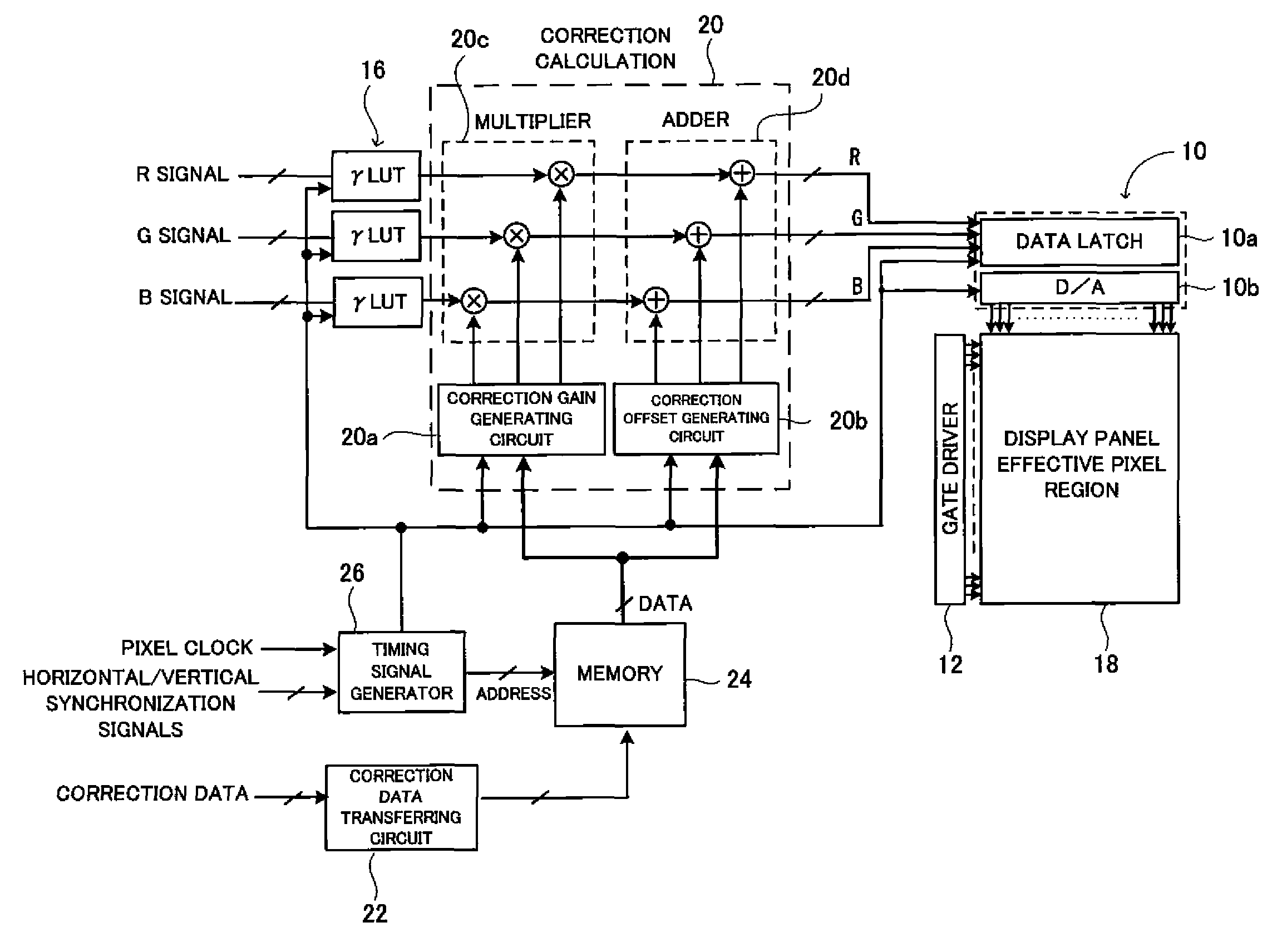
[0046]A preferred embodiment of the present invention will now be described with reference to the drawings. FIG. 4 is a diagram showing an overall structure of a display device. As shown, in the present embodiment, a γ correction circuit (γLUT) 16 is provided so that the image data and the brightness are in a linear relationship, and at the same time, a correction calculating unit 20 is provided so that μ is corrected (gain correction) by multiplying signal data which drives each pixel by a certain value and Vth is corrected (offset correction) by adding a certain value.

[0047]An image data signal is a signal representing brightness of each pixel, and because the signal is a color signal, the image data signal includes image data signals for the colors. Therefore, three γ correction circuits 16 are provided corresponding to the colors of R, G, and B, and γ-corrected image data signals are output from the γcorrection circuits 16. The correction calculating unit 20 applies corrections ...


PUM


Abstract

Displaying an image with unevenness correction by measuring Vgs-Id characteristics of the transistors in a subset of pixels; approximating each characteristic using an equation of the formId=(a(Vgs−b))c;calculating a value c′ using the approximations; measuring the characteristics of the remaining pixels; approximating each of those characteristics by an equation of the same form, using c′ as the power for all of the approximations, calculating corrected image signals for each pixel using the respective approximations of the corresponding pixels of the display device to correct for unevenness; and applying the corrected image signals to the corresponding pixels of the display device to display a corresponding image with unevenness correction.

Description

CROSS-REFERENCE TO RELATED APPLICATION[0001]This application claims priority of Japanese Patent Application No. 2008-106025 filed Apr. 15, 2008 which is incorporated herein by reference in its entirety.FIELD OF THE INVENTION[0002]The present invention relates to unevenness correction data acquisition in an organic electroluminescence (hereinafter referred to as “EL”) display device having an unevenness correcting function which corrects brightness unevenness during display by executing a calculation based on an input signal, and correction data for correcting variation of brightness among pixels during display.[0003]Organic EL display devices which use organic EL elements as light emitting elements are known. In an organic EL element, an amount of emitted light changes depending on the current flowing, and in an active matrix organic EL display device, a thin film transistor (hereinafter referred to as “TFT”) is used for controlling the amount of current.[0004]FIG. 1 shows a basic s...

Claims


Application Information

Patent Timeline
Patent Type & Authority Patents(United States)
IPC IPC(8): G09G3/30
CPCG09G3/3233G09G2320/0285G09G2320/0295
Inventor MIZUKOSHI, SEIICHIKOHNO, MAKOTOONOMURA, KOUICHIMORI, NOBUYUKI
Owner GLOBAL OLED TECH
Why Eureka
Try Eureka