Piezoelectronic device and method of fabricating the same
a technology of electroelectronic devices and carbon nanotubes, which is applied in piezoelectric/electrostrictive/magnetostrictive devices, piezoelectric/electrostriction/magnetostriction machines, etc., can solve the problems of low reliability and short life-span of the electroelectronic device using zinc oxide nanotubes, and achieves good reliability and long life. , the uniformity of the piezoceramic layer covering on
- Summary
- Abstract
- Description
- Claims
- Application Information
AI Technical Summary
Benefits of technology
Problems solved by technology
Method used
Image

Examples
example 1
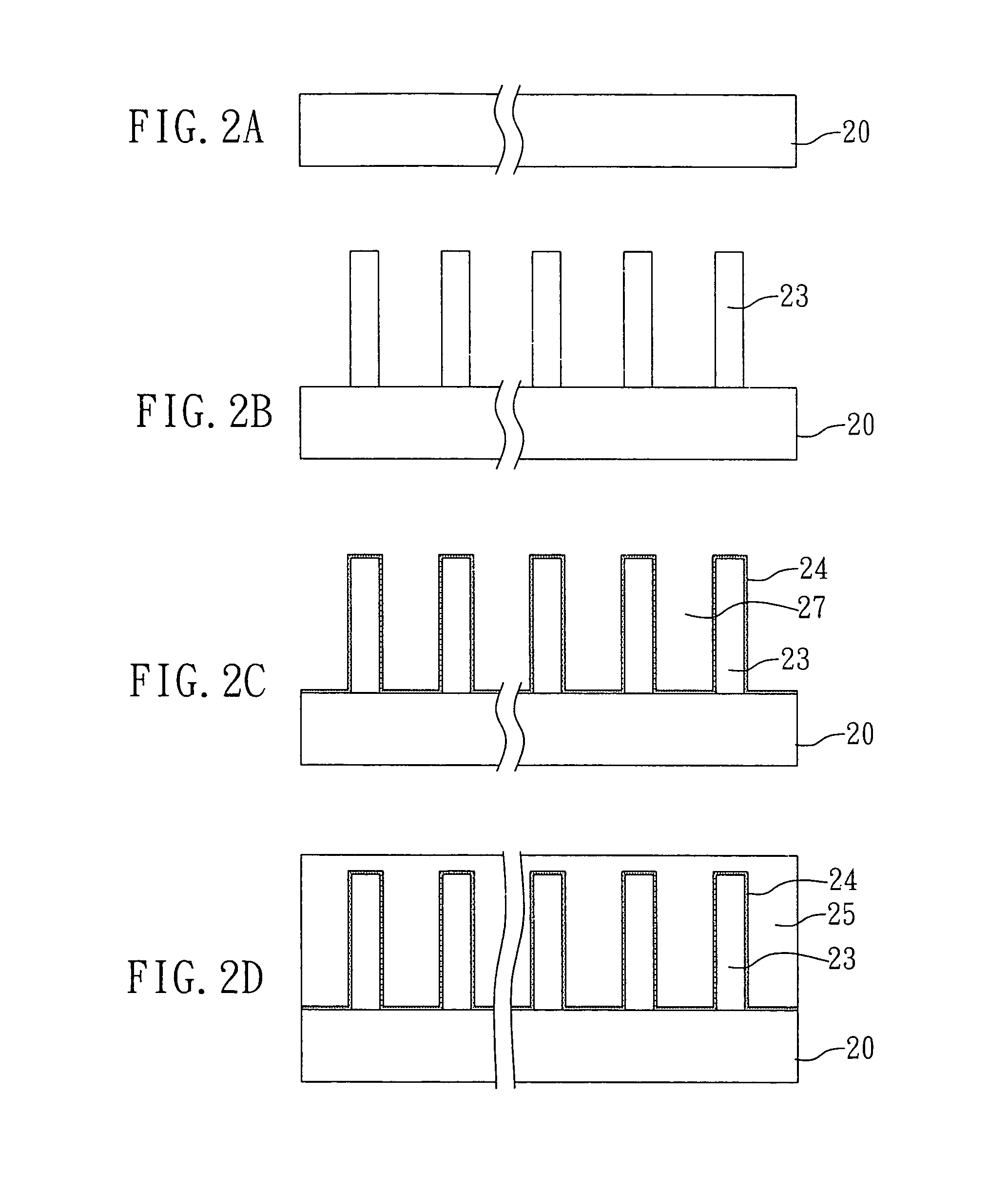
[0054]With reference to FIGS. 2A-2H, a process flow chart of fabricating a piezoelectronic device of the present example is shown. First, (a) a substrate 20 is provided, as shown in FIG. 2A. Then, (b) a plurality of carbon nanotubes 23 is formed on the substrate 20, as shown in FIG. 2B. Herein, the substrate 20 is a silicon-based substrate.
[0055]Then, (c) a zinc oxide layer 24 (i.e. the piezoceramic layer) is formed and covers the plurality of carbon nanotubes 23 by an atomic layer deposition method, as shown in FIG. 2C, and (c0) the atomic layer deposition in the step (c) is repeated for 800 cycles (not shown) to obtain a total thickness of about 640 Å of the zinc Oxide layer.
[0056]Then, (d) a space 27 between the carbon nanotubes 23, which is covered with the at least one piezoceramic layer 24, is filled with a filling material 25 by a thermo evaporation method, as shown in FIGS. 2C and 2D. Herein, parylene is used as the filling material 25. Then, (d1) the filling material 25 is ...
example 2
[0064]With reference to FIGS. 4A-4F, a process flow chart of fabricating a piezoelectronic device of the present example is shown. First, (a) a substrate 20 is provided, as shown in FIG. 4A. Then, (b) a plurality of carbon nanotubes 23 is formed on the substrate 20, as shown in FIG. 4B. Herein, the substrate 20 is a silicon-based substrate.
[0065]Then, (c) a zinc oxide layer 24 is formed and covers the plurality of carbon nanotubes 23 by an atomic layer deposition method, as shown in FIG. 4C, and (c0) the atomic layer deposition in the step (c) is repeated for 800 cycles (not shown) to obtain a total thickness of about 640 Å of the zinc oxide layer.
[0066]Then, (d) a space 27 between the carbon nanotubes 23, which is covered with the at least one piezoceramic layer 24, is filled with a filling material 25 by a vacuum infiltration method, as shown in FIG. 4D. Herein, parylene is used as the filling material 25. Next, (d1) the filling material 25 is plasma etched to expose the plurality...
example 3
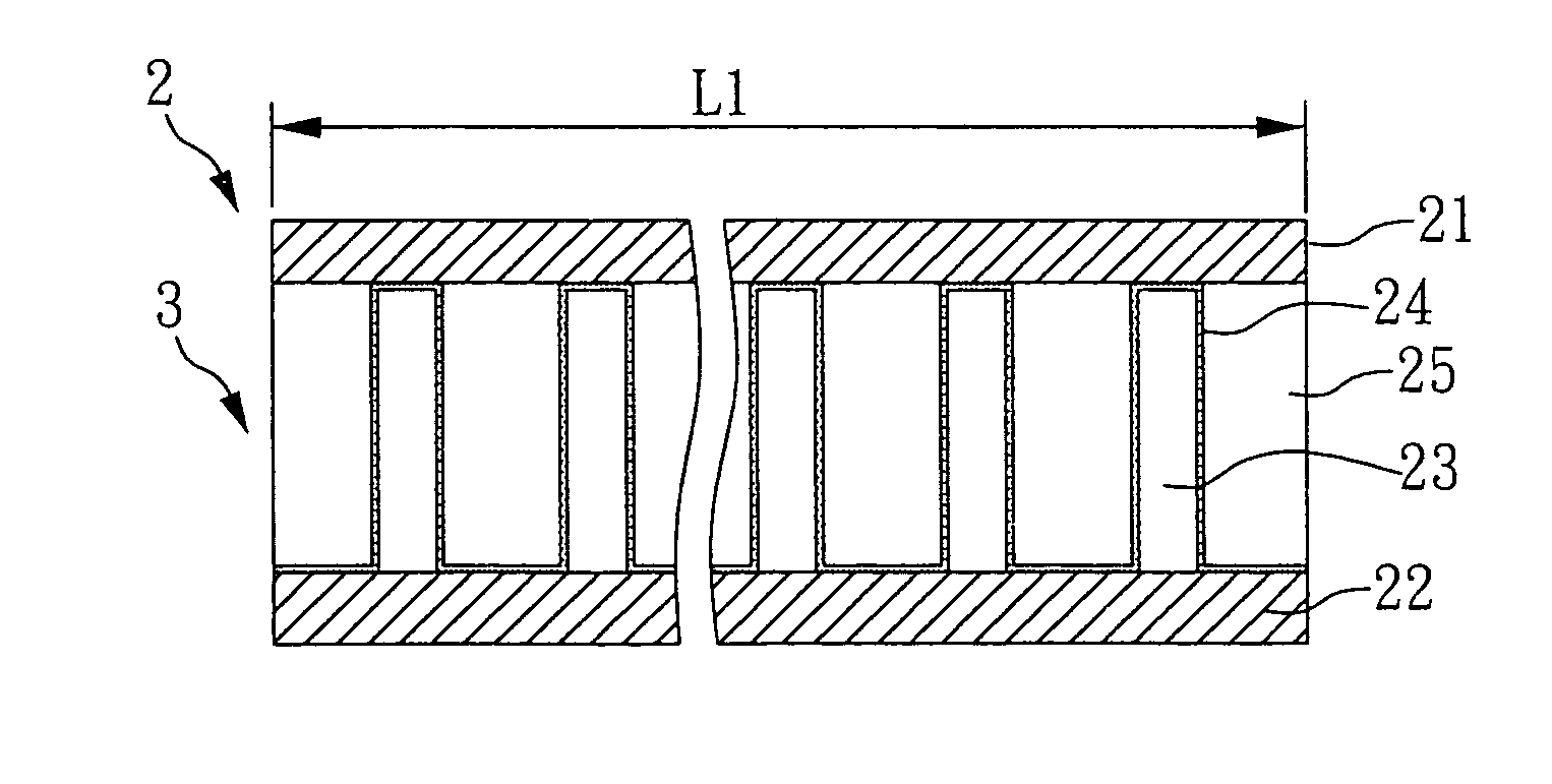
[0069]A piezoelectronic block 3 is provided using the same method as described in the example 2 (steps (a) to (e)), as shown in FIGS. 4A to 4F. Then, as shown in FIG. 5, (f1) a first and a second conductive layer 21 and 22 are respectively formed on the two side surfaces 33 and 34 of the piezoelectronic block 3 and electrically connect with the piezoceramic layer 24.
[0070]Reference with FIG. 5, according to the piezoelectronic device 2 of the present example, the first conductive layer 21, the second conductive layer 22, and the piezoelectronic block 3 are connected in series (i.e. the axial direction of the carbon nanotubes 23 is practically parallel to the surface of the first and the second conductive layers 21,22), and the voltage can be increased to over 1V when the series connecting length L2 of the piezoelectronic device 2 is more than 2.5 mm.
PUM
| Property | Measurement | Unit |
|---|---|---|
| width | aaaaa | aaaaa |
| length | aaaaa | aaaaa |
| length | aaaaa | aaaaa |
Abstract
Description
Claims
Application Information
 - R&D
- Intellectual Property
- Life Sciences
- Materials
- Tech Scout
- Unparalleled Data Quality
- Higher Quality Content
- 60% Fewer Hallucinations
Browse by: Latest US Patents, China's latest patents, Technical Efficacy Thesaurus, Application Domain, Technology Topic, Popular Technical Reports.
© 2025 PatSnap. All rights reserved.Legal|Privacy policy|Modern Slavery Act Transparency Statement|Sitemap|About US| Contact US: help@patsnap.com