Optical module and fabrication method of the same
a technology of optical modules and fabrication methods, applied in the direction of optical waveguide light guides, instruments, applications, etc., can solve the problems of serious bottlenecks in production, increase in the number of optical components used, and significant production problems, so as to improve the productivity and reliability of optical modules, achieve effective and reliable production, and simple alignment
- Summary
- Abstract
- Description
- Claims
- Application Information
AI Technical Summary
Benefits of technology
Problems solved by technology
Method used
Image
Examples
first embodiment
[0069](The First Embodiment)
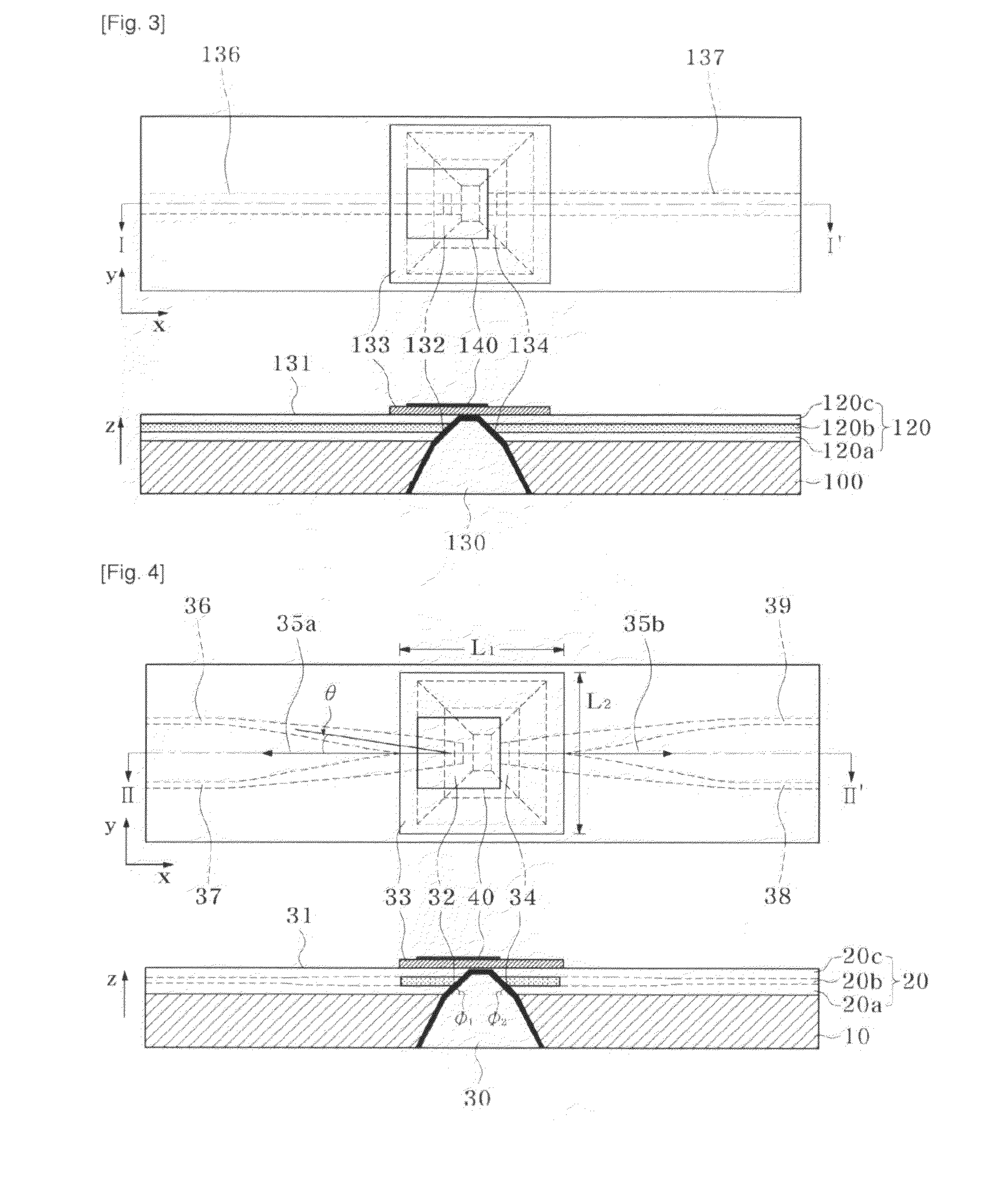
[0070]FIG. 3 is a plan-view and cross-section of the optical module according to the first embodiment of this invention.
[0071]Referring to the FIG. 3, the optical module of the first embodiment comprises an optical waveguide 120 formed on a substrate 100; a cutout 130 with at least two slant surfaces passing at least the core 120b of the optical waveguide with a slant 132; an optical film (not-illustrated) coated optionally on the slant 132; and a film-filter 133 above the cutout 130.
[0072]Referring to the FIG. 3, the optical waveguide 120 comprises the first waveguide 136 on the input side and the second waveguide 137 on the opposite side. But it is also possible to configure an optical module using only one of these 136,137 when necessary. When the optical waveguide 120 has a function of transmitting light through the slants 132,134, it is desirable for the cutout 130 to be filled with a transparent optical media. The slants 132,134 may be a total-inter...
second embodiment
[0080](The Second Embodiment)
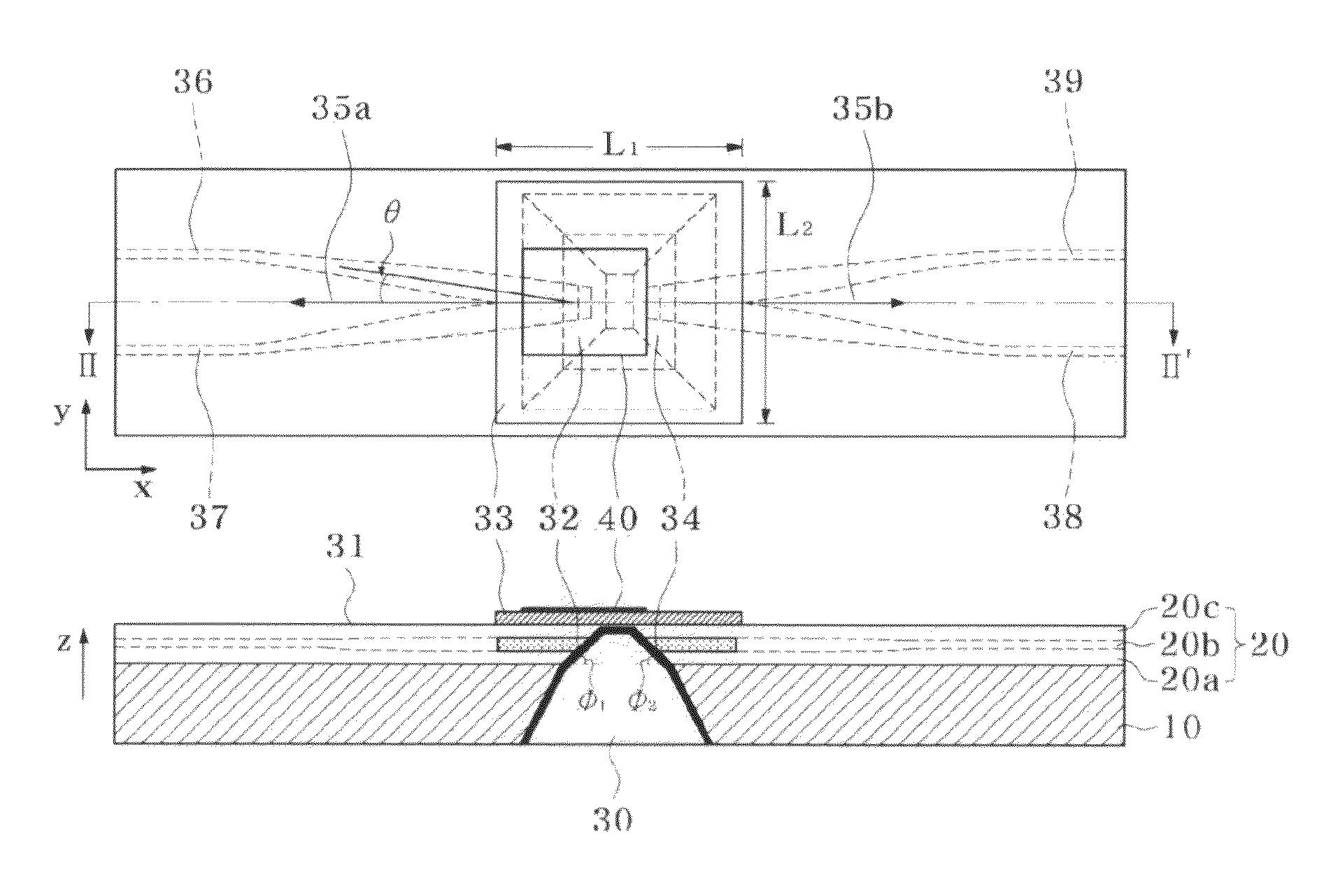
[0081]The FIG. 4 shows the plain-view and the cross-section of the 3-wavelength BiDi optical transceiver employing the principle of this invention.
[0082]Referring to the FIG. 4, the BiDi triplexer according to the second embodiment is furnished with the first and the second optical waveguide 36,37, the third and the fourth optical waveguide 38,39, the cutout 30, and the film-filter 33. Preferably the cutout 30 is filled with an optical media.
[0083]The first and the second optical waveguide 36,37 has a mutually crossing area L1,L2 on the substrate 10; and the third and the fourth optical waveguide 38,39 are connected to each of the first and the second optical waveguide 36,37 through the crossing area L1,L2.
[0084]The cutout 30 is formed in the crossing area L1,L2, and is furnished with the first slant 32 cutting the first and the second optical waveguide 36,37 with a first cutting angle (Φ1) and the second slant 34 cutting the third and the fourth optical...
fifth embodiment
[0103]It is worthwhile to mention that the films on the first 32 and the second slant 34 of the cutout 30 can be coated at a different ratio by depositing at an inclined angle. In this case, the stacked films on each side of the slants 32,34 has a fixed ratio in theirs thicknesses, depending on the inclined angle, which results in some shift in the spectral window of reflection or transmission. Using this method, the optical characteristics of the first 32 and the second slant 34 from a single pattern of a cutout can be tuned differently. This method of tuning is applied in the
[0104]The third optical waveguide 38 in direction of piercing the first and the second slant 32,34 is selected for the transmission of 1.31 μm wavelength in reverse direction. On the slant, the filter having good characteristics of wavelength separation is difficult to design, because the angle of slant is close to the Brewster angle, hence resulting in a significant dependence of reflection or transmission on...
PUM
 Abstract
Description
Claims
Application Information


