Optical Module and Fabrication Method of the Same

a technology applied in the field of optical modules and fabrication methods of the same, can solve the problems of serious bottleneck in production, increase in the number of optical components used, and significant production problems, and achieve the effects of improving the productivity and reliability of optical modules, facilitating the production of effective and reliable methods, and simple alignmen

Inactive Publication Date: 2010-06-03
CHUNG KYOUNG HIE
View PDF16 Cites 44 Cited by
  • Summary
  • Abstract
  • Description
  • Claims
  • Application Information

AI Technical Summary

Benefits of technology

[0050](1) Optical signals of specific wavelengths can be separated out from the optical waveguide or combined into the optical waveguide either forward or reverse direction of the optical waveguide.
[0051](2) Using this invention, highly efficient bi-directional multi-port multi-wavelength optical transceivers which is simple to align its component elements can be effectively and reliably produced from the front and back side of the wafer through a wafer-level process: Such a wafer-level process produces simultaneously hundreds of optical waveguides, film-filters, plurality of optical surfaces which are necessary for combining or splitting the wavelength of the optical signals excluding the one-by-one process for each device.
[0052](3) The productivity and reliability of the optical module can be improved in a jump by coating the optical films on the wafer surface instead of inserting discrete films one by one into grooves and fixing these using an epoxy as in a traditional way.
[0053](4) The performances of each kinds of optical films can be optimized: The film-filters on the wafer surface are used for separating or combining the closely spaced wavelengths as the receiving channels of 1.49□ and 1.55□ in the triplexer, and the optical film on the first slant is used for separating or combining the sparsely spaced wavelengths as the transmitting channel of 1.31□ in the triplexer into the reverse path of receiving, standing apart from 1.49□. In other word, the polarization dependence in the separation of closely-spaced wavelength channels can be improved by adopting a structure of crossing waveguide with a slant, where the crossing angle can be chosen small as desired within the range of preventing the cross-talk between the waveguides.
[0054](5) The size of the optical module is reduced: One unit of a cross-waveguide has three optical sets of films with four waveguide and two optical devices on top and bottom of the substrate, which enables a compact structure as shown in the embodiment of triplexer.

Problems solved by technology

As the number of wavelength channel in use increases in this manner, the number of optical components in use increases and the optical alignments in the assembly of the components becomes a critical issue in the production of device.
In case of BiDi triplexer, for example, the optical alignment using the former technology has about 50 freedoms to fix in the alignment; and consequently one assembly of the device takes more than 10 minutes resulting in a serious bottleneck of production.
This involves still a significant problem in production even though there is some improvement compared to the former methods of using the filter in free space as in the FIG. 1.
While the patent “OPTICAL COMPONENT FOR FREE-SPACE OPTICAL PROPAGATION BETWEEN WAVEGUIDES” (U.S. Pat. No. 7,031,575 B2, Xponent Photonics Inc.) also releases a module similar to the method in the FIG. 2, but this method still involves similar problem of inserting thin films into grooves encountered previously in the production of the devices.

Method used


Image

  • Optical Module and Fabrication Method of the Same
  • Optical Module and Fabrication Method of the Same
  • Optical Module and Fabrication Method of the Same

Examples


first embodiment

The First Embodiment

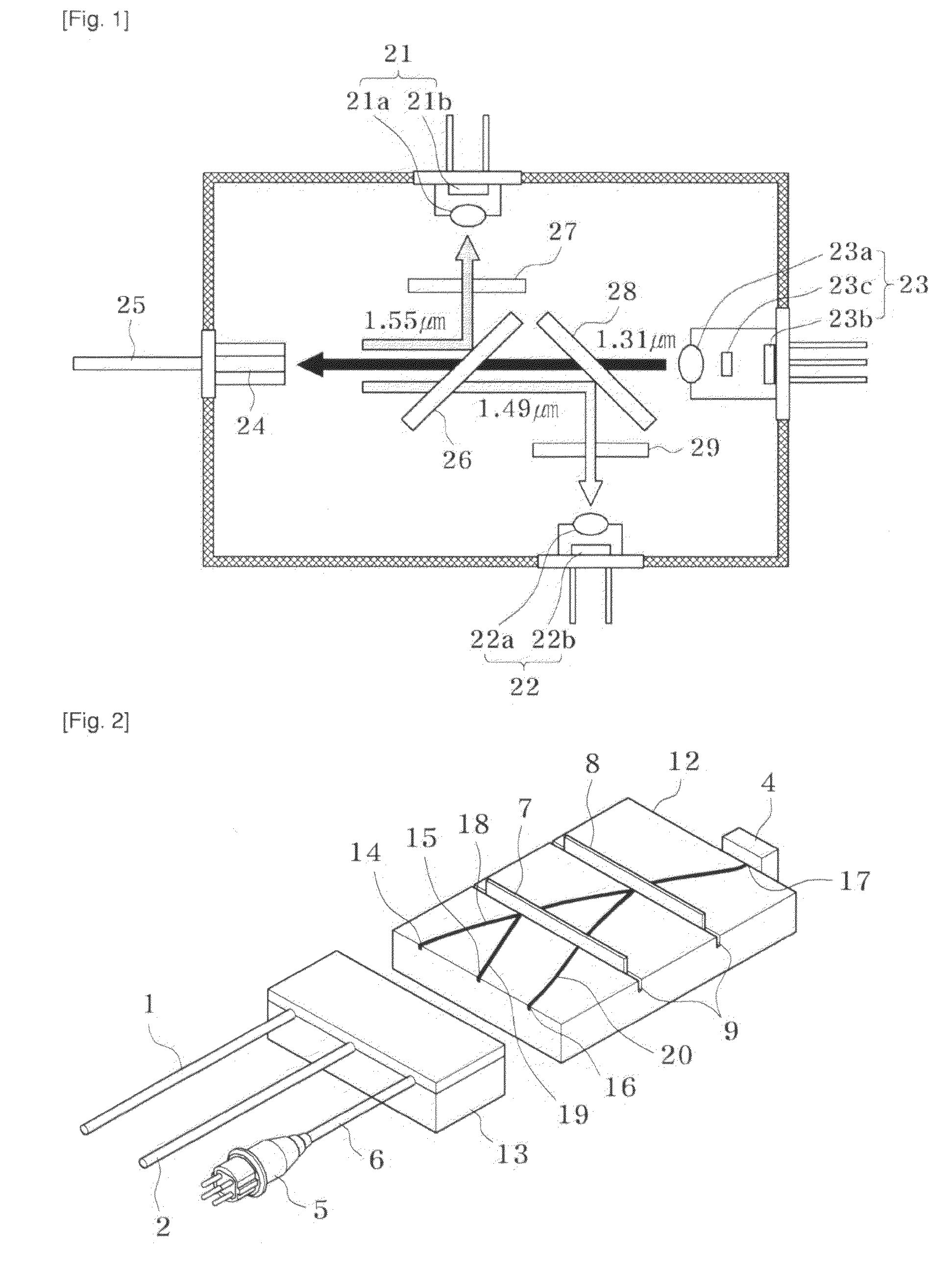
[0069]FIG. 3 is a plan-view and cross-section of the optical module according to the first embodiment of this invention.

[0070]Referring to the FIG. 3, the optical module of the first embodiment comprises an optical waveguide 120 formed on a substrate 100; a cutout 130 with at least two slant surfaces passing at least the core 120b of the optical waveguide with a slant 132; an optical film (not-illustrated) coated optionally on the slant 132; and a film-filter 133 above the cutout 130.

[0071]Referring to the FIG. 3, the optical waveguide 120 comprises the first waveguide 136 on the input side and the second waveguide 137 on the opposite side. But it is also possible to configure an optical module using only one of these 136,137 when necessary. When the optical waveguide 120 has a function of transmitting light through the slants 132,134, it is desirable for the cutout 130 to be filled with a transparent optical media. The slants 132,134 may be a total-internal refl...

second embodiment

The Second Embodiment

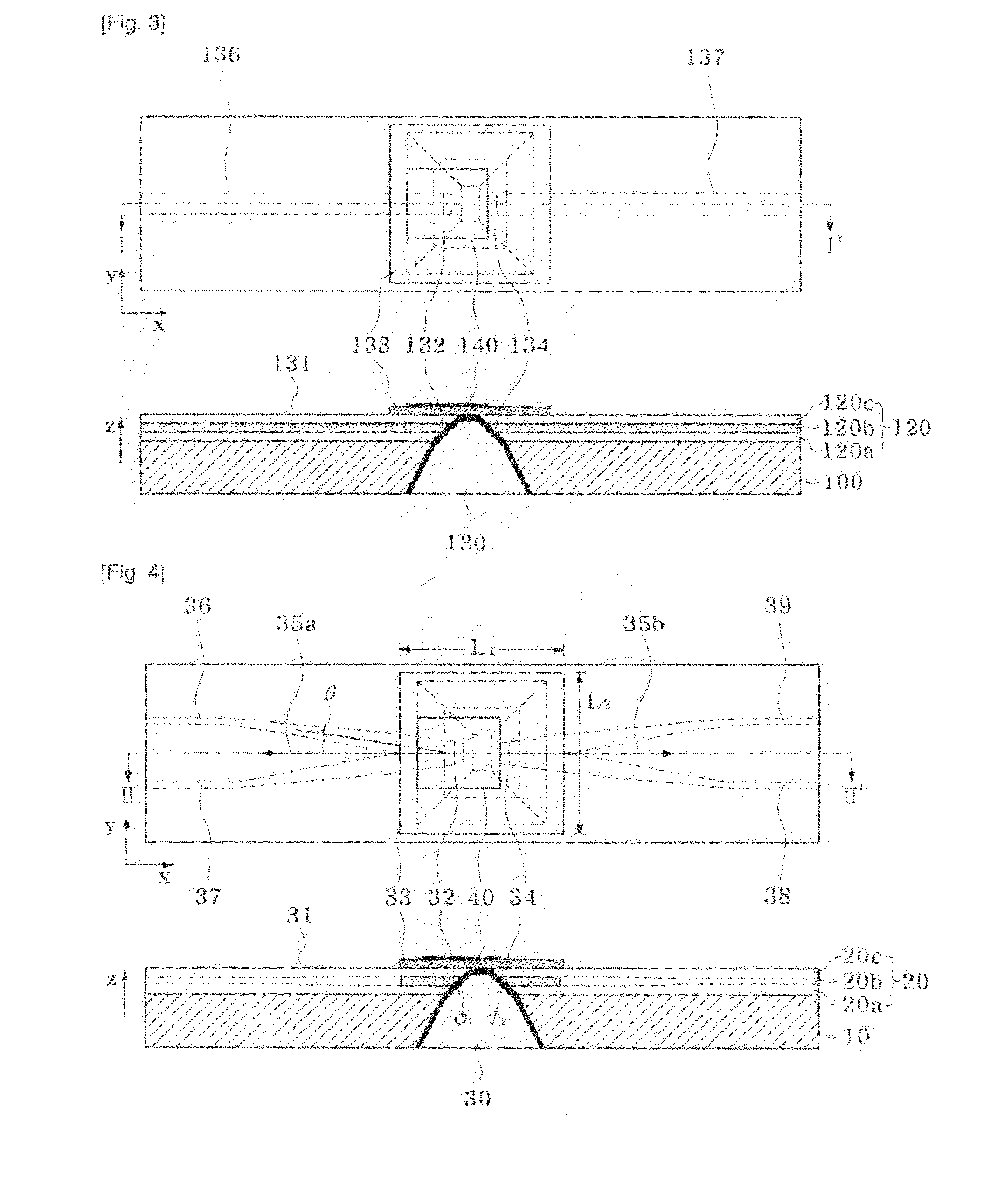
[0079]The FIG. 4 shows the plain-view and the cross-section of the 3-wavelength BiDi optical transceiver employing the principle of this invention.

[0080]Referring to the FIG. 4, the BiDi triplexer according to the second embodiment is furnished with the first and the second optical waveguide 36,37, the third and the fourth optical waveguide 38,39, the cutout 30, and the film-filter 33. Preferably the cutout 30 is filled with an optical media.

[0081]The first and the second optical waveguide 36,37 has a mutually crossing area L1,L2 on the substrate 10; and the third and the fourth optical waveguide 38,39 are connected to each of the first and the second optical waveguide 36,37 through the crossing area L1, L2.

[0082]The cutout 30 is formed in the crossing area L1,L2, and is furnished with the first slant 32 cutting the first and the second optical waveguide 36,37 with a first cutting angle (Φ1) and the second slant 34 cutting the third and the fourth optical wavegu...

third embodiment

The Third Embodiment

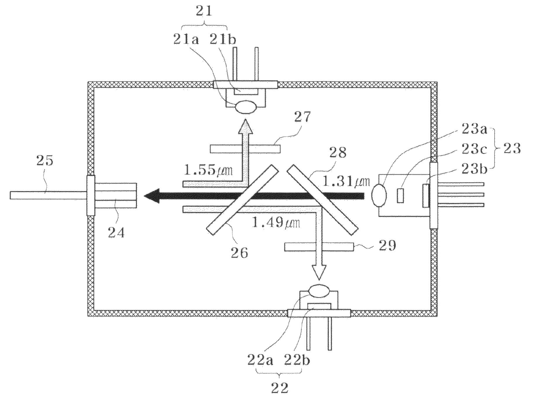
[0120]FIG. 10 is the schematic layout of 4-wavelength optical transceiver produced applying the optical module in this invention. Each component module 56,57,58,59,60 in the FIG. 10 represents the optical module in this invention as in the FIG. 3. The unit modules 56,57,58,59,60 are furnished with the film-filters 56a,57a,58a,59a,60a, optical devices 56b,57b,58b,59b,60b, and the cutouts with the slants (not-illustrated)

[0121]The 4-wavelength optical transceiver in the third embodiment has the receiving wavelengths of 1.49 μm, 1.55 μm, and 1.61 μm, and the transmitting wavelength of 1.31 μm. The IO (Input-output) port 51a of optical signal to external is connected to the first unit of optical module 56 through the optical waveguide 51. The first unit of module 56 receives one channel of wavelength and combines one channel of transmission wavelength into the reverse direction of the incoming optical path. The second and the third unit of module 57,58 connected by t...


PUM

PropertyMeasurementUnit
cutting angleaaaaaaaaaa
incidence angleaaaaaaaaaa
θaaaaaaaaaa

Abstract

Disclosed is an optical module comprising, an optical waveguide on the upper side of a substrate; a cutout with at least two slant surfaces, passing at least the core of the optical waveguide; and a film-filter above the cutout. Constructions of bi-directional multi-wavelength optical transmitter-receiver assembly using the optical module as a unit element are also provided in variety on a planar substrate. According to this invention, a bi-directional multi-wavelength transmitter-receiver, which is compact, reliable, excellent in the optical performance and simple in the alignments between the composing elements, can be produced.

Description

TECHNICAL FIELD [0001]The present invention is related to c and method thereof. The optical module comprises an optical waveguide, at least one slanted surface, and film filters on a planar substrate. Constructions of bi-directional multi-wavelength optical transmitter-receiver assembly using the optical module as a unit element are also provided in variety on a planar substrate. According to this invention, a bi-directional multi-wavelength transmitter-receiver, which is compact, reliable, excellent in the optical performance and simple in the alignments between the composing elements, can be produced.BACKGROUND ART[0002]Bi-directional optical communication transmits and receives simultaneously optical signals in both directions of a single optical fiber. In each direction, the optical wavelength in use is different, which provides two independent path of communication even if the path is single. Consequently, at the end of an optical fiber, the optical signal of outgoing is to be ...

Claims


Application Information

Patent Timeline
Patent Type & Authority Applications(United States)
IPC IPC(8): G02B6/36B29D11/00
CPCG02B6/12007G02B6/1228G02B6/29361G02B6/4246G02B6/4214G02B6/4215G02B6/42G02B6/10
Inventor CHOI, JUN SEOKLEE, HYUNG JONG
Owner CHUNG KYOUNG HIE
Why Eureka
Try Eureka