Scalable scan system for system-on-chip design

a scan system and system-on-chip technology, applied in memory systems, error detection/correction, instruments, etc., can solve the problems of not allowing scan testing to be performed through memory arrays, requiring extensive and time-consuming changes, and introducing extra scan blocks or chains during the end stages of the design

Inactive Publication Date: 2011-09-27
INTEL CORP
View PDF6 Cites 14 Cited by
  • Summary
  • Abstract
  • Description
  • Claims
  • Application Information

AI Technical Summary

Problems solved by technology

However, for the design of the prior art system-on-chip 105, scan insertion poses a potential problem as the current scan insertion techniques are not scalable and any addition of extra scan blocks or chains during the end stages of the design requires extensive and time-consuming changes.
The scan flip-flops inserted to bypass the memory arrays not only require additional chip area, they also do not allow scan testing to be performed through the memory arrays.

Method used


Image

  • Scalable scan system for system-on-chip design
  • Scalable scan system for system-on-chip design
  • Scalable scan system for system-on-chip design

Examples


Embodiment Construction

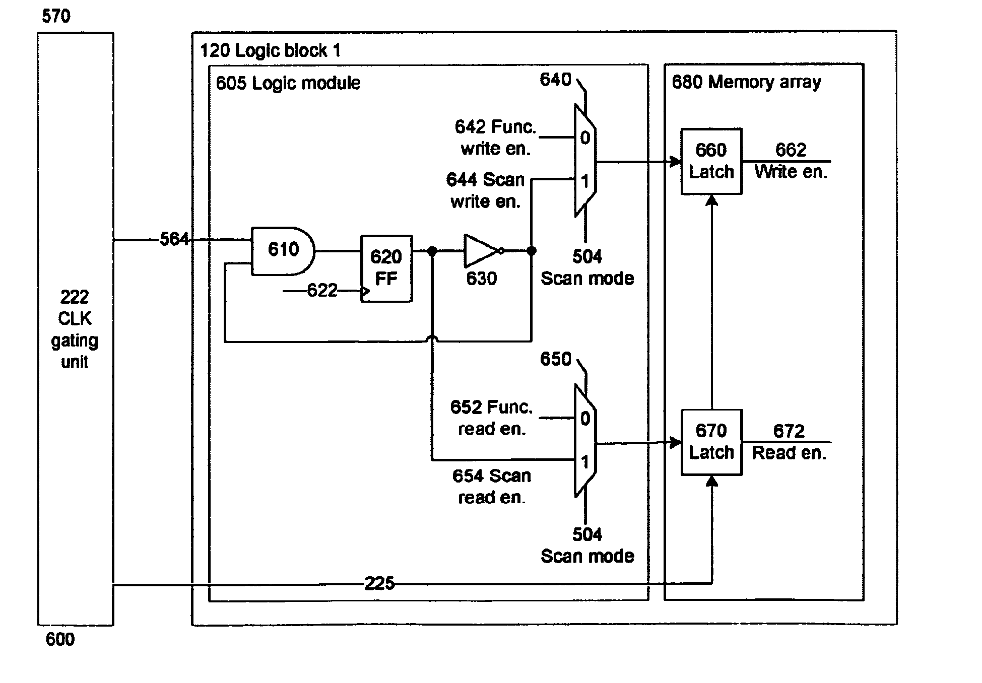
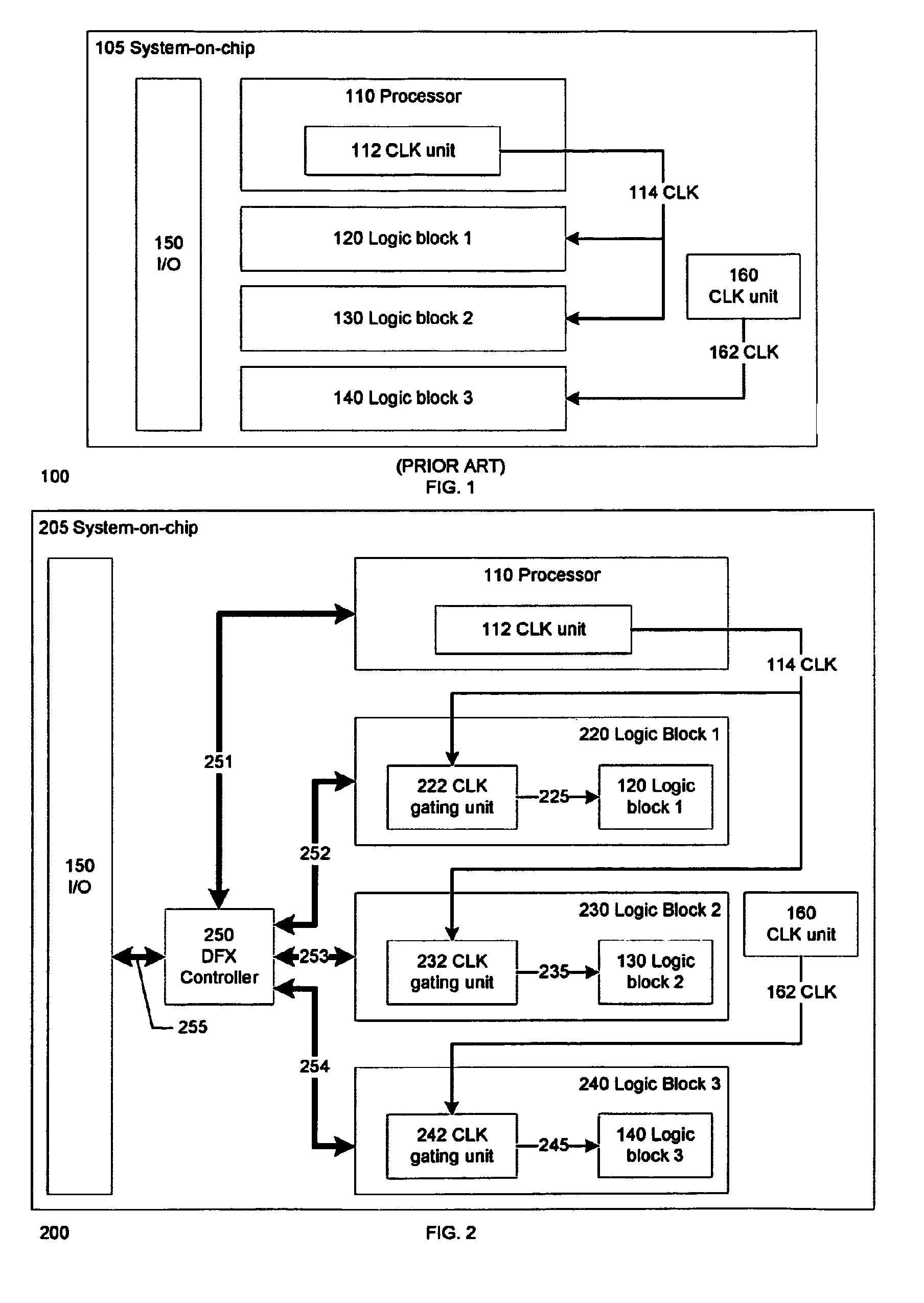
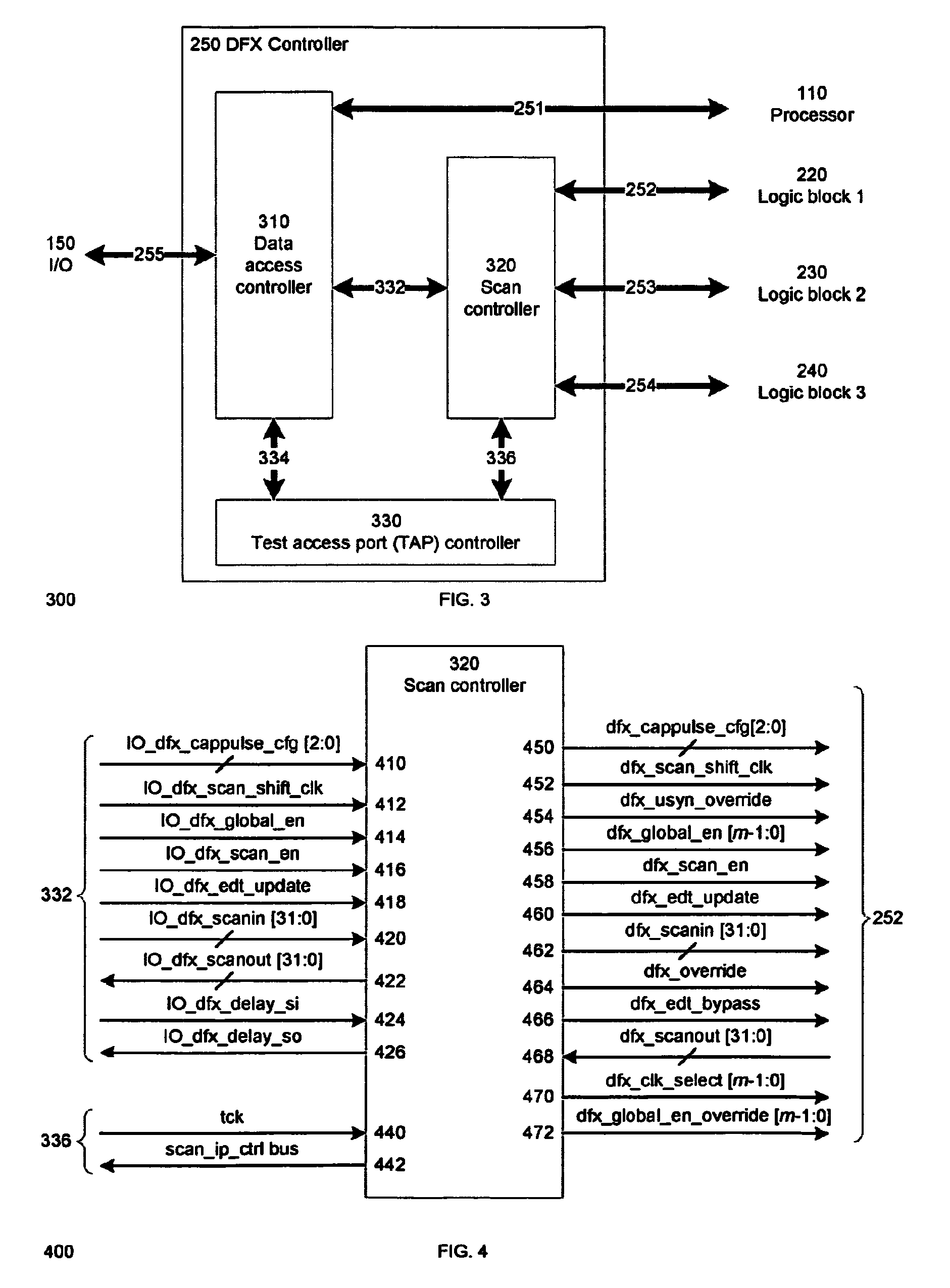
[0015]Embodiments of the invention described herein are illustrated by way of example and not by way of limitation in the accompanying figures. For simplicity and clarity of illustration, elements illustrated in the figures are not necessarily drawn to scale. For example, the dimensions of some elements may be exaggerated relative to other elements for clarity. Further, where considered appropriate, reference numerals have been repeated among the figures to indicate corresponding or analogous elements. Reference in the specification to “one embodiment” or “an embodiment” of the invention means that a particular feature, structure, or characteristic described in connection with the embodiment is included in at least one embodiment of the invention. Thus, the appearances of the phrase “in one embodiment” in various places throughout the specification are not necessarily all referring to the same embodiment.

[0016]Embodiments of the invention provide a method and system to facilitate a ...


PUM


Abstract

A method and system to facilitate a scalable scan system in the design of a system-on-chip. In one embodiment of the invention, the system-on-chip includes a controller and one or more clock gating units. The clock gating unit is added to each unique clock domain of each function or logic block in the system-on-chip. By having a controller that connects to each clock gating unit and the scan input and output signals in each logic block of the SOC, this allows a scalable scan system in the design of the SOC and allows frequent block level design changes in the SOC without extensive changes to the scan logic in one embodiment of the invention. In addition, the scalable scan system also allows at-speed scan write-through testing of a memory array that can improve the scan test coverage of the system-on-chip.

Description

FIELD OF THE INVENTION[0001]This invention relates to a system-on-chip, and more specifically but not exclusively, to a scalable scan system for a system-on-chip design.BACKGROUND DESCRIPTION[0002]In the design of a system-on-chip, there are several design methodologies such as design for test (DFT), design for manufacturing (DFM), and design for debug (DFD), collectively known as DFX, for example, that can be used to increase the testability, fault coverage and manufacturing yield of the system-on-chip. Scan insertion, or the conversion of flip-flops into scan flip-flops to form scan chains, is a common technique used in digital integrated circuit design to allow production testers to check for any manufacturing faults of the integrated circuit using the aid of the scan chains.[0003]FIG. 1 illustrates a block diagram 100 of a prior art system-on-chip 105. The prior art system-on-chip 105 has a processor 110 with a clock (CLK) unit 112 that provides a CLK 114 to the logic block 1120...

Claims


Application Information

Patent Timeline
Patent Type & Authority Patents(United States)
IPC IPC(8): G01R31/28
CPCG01R31/318552G06F11/2733G11C29/32G11C2029/3202
Inventor LI, WEILIN, CHIH-JEN M.SATHYANARAYANAN, PRAVEEN
Owner INTEL CORP
Why Eureka
Try Eureka