Methods for planarizing unevenness on surface of wafer photoresist layer and wafers produced by the methods

a technology of photoresist layer and method, which is applied in the field of method of planarizing unevenness on the surface of a photoresist layer of a wafer and also to a wafer, can solve problems such as esc cleaning, and achieve the effects of reducing esc cleaning, improving esc life, and improving uniformity and repeatability

Active Publication Date: 2011-12-06
FUNAI ELECTRIC CO LTD
View PDF8 Cites 1 Cited by
  • Summary
  • Abstract
  • Description
  • Claims
  • Application Information

AI Technical Summary

Benefits of technology

[0015]Underlying the innovation of the present invention is the insight by the inventors herein that a peripheral edge bead can be removed from a photoresist edge stop by using the gray-scale lithography technique alone, and thus without use of the DRIE technique, to substantially planarize the surface of the etch stop without disturbance of the wafer substrate. While the use of this gray-scale lithography technique adds a process step and may require modifications to some current steps, the disadvantages of any such additions and modifications are more than offset by the substantial benefits that are gained, such as improved, more uniform and repeatable cooling, reduced ESC cleaning (the source of significant downtime), extended ESC life due to reduced cleanings, and improved DRIE uptime.

Problems solved by technology

While the use of this gray-scale lithography technique adds a process step and may require modifications to some current steps, the disadvantages of any such additions and modifications are more than offset by the substantial benefits that are gained, such as improved, more uniform and repeatable cooling, reduced ESC cleaning (the source of significant downtime), extended ESC life due to reduced cleanings, and improved DRIE uptime.

Method used


Image

  • Methods for planarizing unevenness on surface of wafer photoresist layer and wafers produced by the methods
  • Methods for planarizing unevenness on surface of wafer photoresist layer and wafers produced by the methods
  • Methods for planarizing unevenness on surface of wafer photoresist layer and wafers produced by the methods

Examples


Embodiment Construction

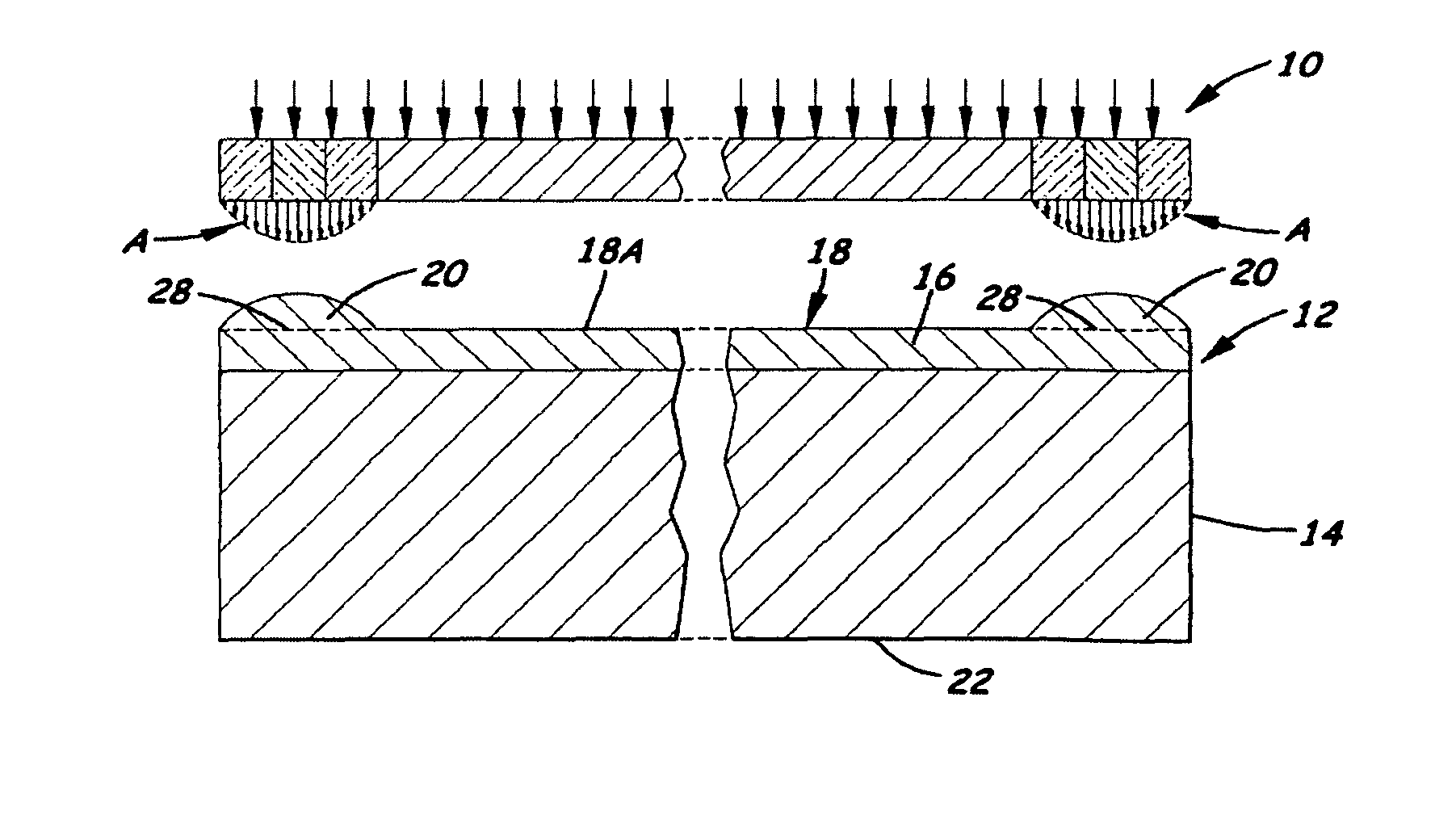
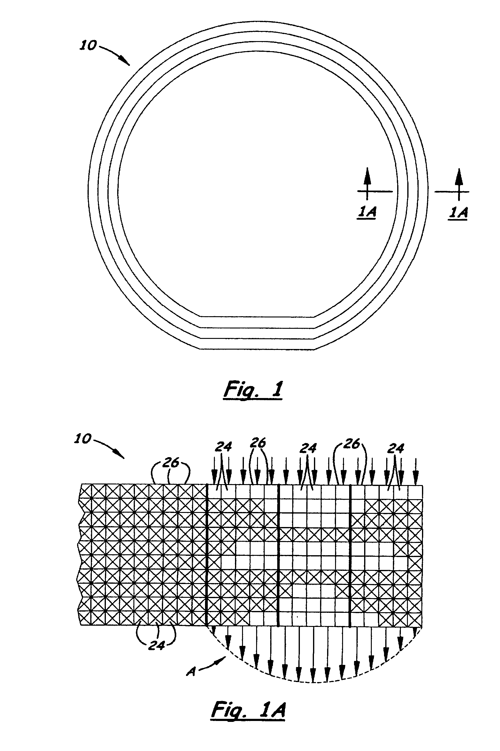
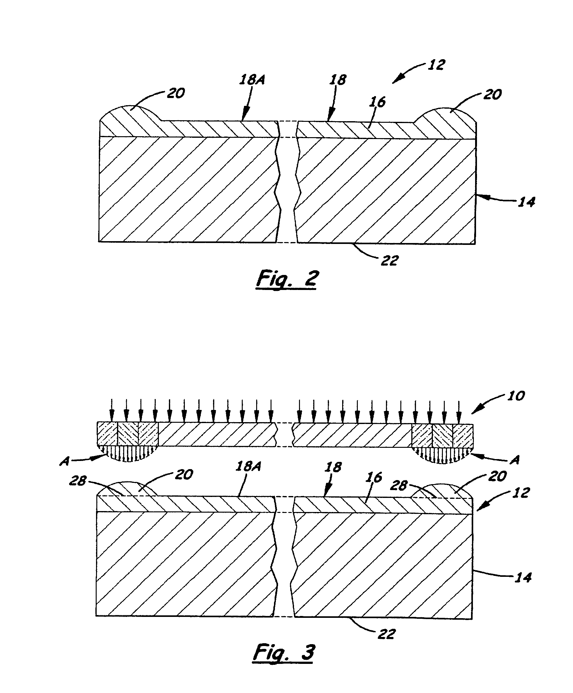
[0024]The present invention now will be described more fully hereinafter with reference to the accompanying drawings, in which some, but not all embodiments of the invention are shown. Indeed, the invention may be embodied in many different forms and should not be construed as limited to the embodiments set forth herein; rather, these embodiments are provided so that this disclosure will satisfy applicable legal requirements. Like numerals refer to like elements throughout the views.

[0025]As mentioned earlier, in a typical application as used heretofore, the gray-scale lithography technique is employed in combination with a DRIE technique. This prior art combination is disclosed in U.S. Pat. No. 5,310,623 to Gal, International patent application publication WO 02 / 31600 (also PCT / US01 / 426290 to Whitney et al., and an article entitled “Microfabrication of 3D silicon MEMS structures using gray-scale lithography and deep reactive ion etching” by C. M. Waits et al. Sensors and Actuators ...


PUM

PropertyMeasurementUnit
optical densitiesaaaaaaaaaa
widthaaaaaaaaaa
widthaaaaaaaaaa

Abstract

A wafer has a substrate and a photoresist layer thereon with a surface that is planarized by positioning over a starting surface of the photoresist layer a gray-scale mask having a pattern that correlates with a gradient height profile of unevenness present on the starting surface, patterning the photoresist layer using the gray-scale mask to produce the pattern thereof in the photoresist layer which, in effect, produces a profile of evenness in the photoresist layer underlying the gradient height profile of unevenness, and developing the patterned photoresist layer such that only a three-dimensional portion thereof corresponding to the gradient height profile of unevenness located above the profile of evenness is removed which, in effect, leaves behind a resulting surface on the photoresist layer made substantially more even and thus substantially in a planarized condition.

Description

CROSS REFERENCES TO RELATED APPLICATIONS[0001]This patent application is related to the U.S. patent application Ser. No. 11 / 562,081, filed Nov. 21, 2006, entitled “Method And Apparatus For Maximizing Cooling For Wafer Processing” and assigned to the assignee of the present application.BACKGROUND[0002]1. Field of the Invention[0003]The present invention relates generally to wafer processing methods and, more particularly, to a method for planarizing unevenness on a surface of a wafer photoresist layer and also to a wafer produced by the method[0004]2. Description of the Related Art[0005]Micro-fluid ejection heads are useful for ejecting a variety of fluids including inks, cooling fluids, pharmaceuticals, lubricants and the like. One use of micro-fluid ejection heads is in an ink jet printer. Ink jet printers continue to be improved as the technology for making the micro-fluid ejection heads continues to advance. New techniques are constantly being developed to provide low cost, highl...

Claims


Application Information

Patent Timeline
Patent Type & Authority Patents(United States)
IPC IPC(8): G03F7/26
CPCG03F7/094
Inventor BERNARD, DAVID LAURIERDRYER, PAUL WILLIAMMCNEES, ANDREW LEE
Owner FUNAI ELECTRIC CO LTD
Why Eureka
Try Eureka