Leadless integrated circuit package having electrically routed contacts

a leadless, integrated circuit technology, applied in the direction of electrical equipment, semiconductor devices, semiconductor/solid-state device details, etc., can solve the problems of limited pcb space, disadvantageous increase in size, and tend to significantly increase the size of ic packages, etc., to achieve high density contacts

Active Publication Date: 2011-12-06
KAIXIN INC
View PDF59 Cites 121 Cited by
  • Summary
  • Abstract
  • Description
  • Claims
  • Application Information

AI Technical Summary

Problems solved by technology

Oftentimes, the presence of external leads tends to significantly increase the size of IC packages.
This increased size can be disadvantageous in systems where PCB space is limited.
In addition, because the external leads are typically arranged along the sides of the IC packages, the pin count of the IC packages is limited by the linear distance around the IC packages.
Another disadvantage is that these leads require an additional inspection step for straightness, co-planarity, and other required mechanical dimensions (and rework or scrap if they fail the specification).
One limitation of this type of leadless IC package is that the maximum number of terminals that can be utilized to pass electrical signals to and from the I / O ports of the IC chip is limited to the number of terminals that can be located around the perimeter of the DAP.
However, increasing the number of rows of terminals requires either decreasing the size of the IC chip or increasing the size of the IC package.
Additionally, the amount the distance between the terminals can be reduced is limited to the minimum distance between connection points on the PCB, which is relatively large.

Method used


Image

  • Leadless integrated circuit package having electrically routed contacts
  • Leadless integrated circuit package having electrically routed contacts
  • Leadless integrated circuit package having electrically routed contacts

Examples


Embodiment Construction

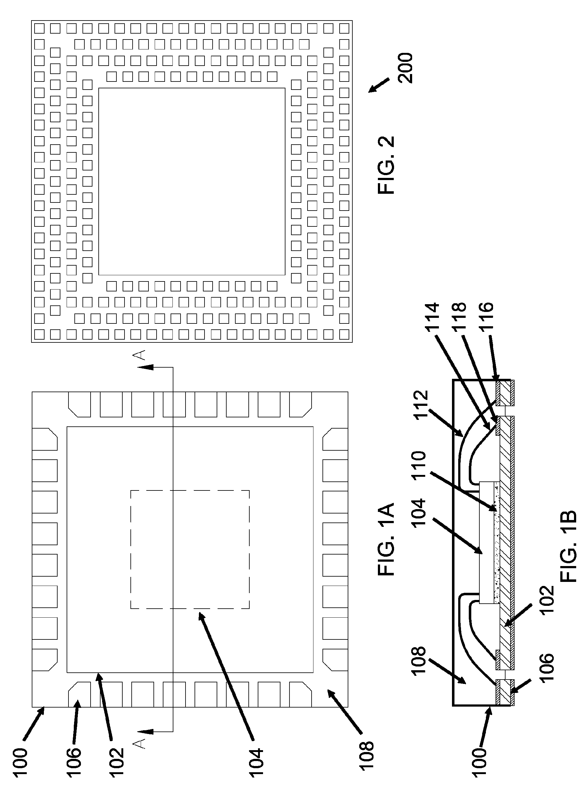
[0036]Various embodiments of the present invention will now be described more fully with reference to the accompanying drawings. The invention may, however, be embodied in many different forms and should not be construed as limited to the embodiments set forth herein; rather, the embodiments are provided so that this disclosure will be thorough and complete, and will fully convey the scope of the invention to those skilled in the art.

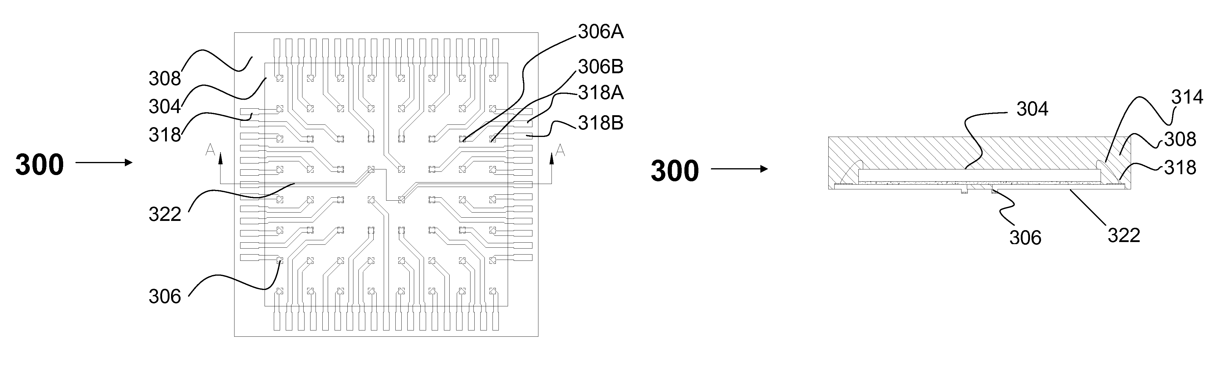
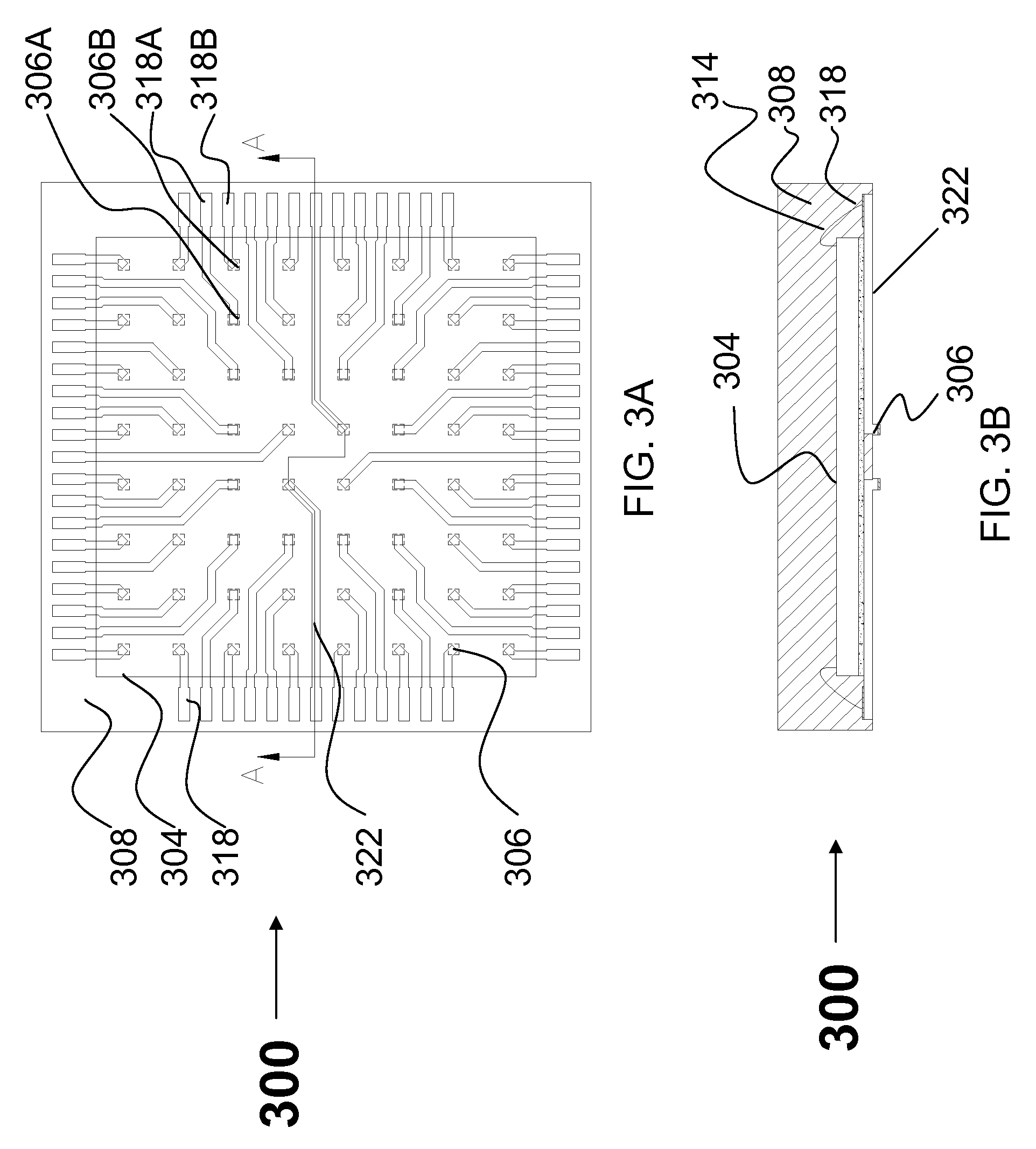
[0037]Referring now to FIGS. 3A-B, two views of an embodiment of a leadless IC package 300 are shown. FIG. 3A is a top view of the IC package 300 before encapsulation and FIG. 3B is a side view of a cross section of the IC package 300 of FIG. 3A along line A-A. In the embodiment shown in FIG. 3B, the IC package 300 includes an IC chip 304 disposed in a central portion of the IC package 300 and covered by an encapsulation compound 308 and adapted to be electrically coupled to an external device (not shown), such as a PCB, through a plurality of terminals...


PUM


Abstract

A leadless integrated circuit (IC) package comprising an IC chip mounted on a metal leadframe and a plurality of electrical contacts electrically coupled to the IC chip. The IC chip, the electrical contacts, and a portion of the metal leadframe are covered with an encapsulation compound, with portions of the electrical contacts exposed on a bottom surface of the encapsulation compound. The electrical contacts of the IC package having metal traces connecting bonding areas on a top surface thereof and contact areas on a bottom surface thereof, wherein at least some of the bonding areas are laterally disposed from the contact areas connected thereto.

Description

CROSS-REFERENCE TO RELATED APPLICATIONS[0001]This patent application claims priority to U.S. Provisional Patent Application Ser. Nos. 61 / 158,170, filed 6 Mar. 2009, and 61 / 166,547, filed 3 Apr. 2009, both of which are hereby incorporated by reference. This patent application is a continuation of PCT Application No. PCT / CN2009 / 072030, filed 27 May 2009, which claims priority to U.S. Provisional Patent Application Ser. Nos. 61 / 158,170, filed 6 Mar. 2009, and 61 / 166,547, filed 3 Apr. 2009.BACKGROUND[0002]1. Technical Field[0003]This patent application relates generally to integrated circuit (IC) packaging technology and, in particular, but not by way of limitation, to leadless IC packages having high density contacts and related methods of manufacture.[0004]2. Background[0005]IC packaging is one of the final stages involved in the fabrication of IC devices. During IC packaging, one or more IC chips are mounted on a package substrate, connected to electrical contacts, and then coated wi...

Claims


Application Information

Patent Timeline
Patent Type & Authority Patents(United States)
IPC IPC(8): H01L23/495H01L21/60
CPCH01L21/78H01L21/4832H01L23/3107H01L23/3121H01L23/49503H01L23/4951H01L23/49541H01L23/49548H01L23/49575H01L23/49582H01L24/49H01L24/97H01L25/0655H01L25/0657H01L24/32H01L2924/00013H01L2924/07802H01L24/29H01L24/45H01L24/48H01L2224/16H01L2224/2919H01L2224/32014H01L2224/32145H01L2224/32245H01L2224/45144H01L2224/48091H01L2224/48095H01L2224/48247H01L2224/48257H01L2224/49171H01L2224/73265H01L2224/85439H01L2224/85444H01L2224/85447H01L2224/97H01L2924/01005H01L2924/01014H01L2924/01027H01L2924/01028H01L2924/01029H01L2924/01033H01L2924/01046H01L2924/01047H01L2924/0105H01L2924/01078H01L2924/01079H01L2924/01082H01L2924/0781H01L2924/09701H01L2924/14H01L2924/15183H01L2924/15311H01L2924/16195H01L2924/19041H01L2924/19043H01L2924/01006H01L2924/01075H01L2924/014H01L2924/0132H01L2225/0651H01L2225/06517H01L2225/06582H01L2225/06506H01L2225/06568H01L2224/29111H01L2224/2929H01L2924/00014H01L2224/85H01L2224/83H01L2924/00H01L2924/0665H01L2224/29099H01L2224/29199H01L2224/29299H01L2224/48639H01L2224/48644H01L2224/48647H01L2924/181H01L2924/00012H01L23/48
Inventor LI, TUNG LOK
Owner KAIXIN INC
Why Eureka
Try Eureka