Semiconductor device
a semiconductor device and metal insulator technology, applied in the direction of semiconductor devices, electrical devices, transistors, etc., can solve the problems of low work function unable to have a eff of about 3.9 to 4.3 ev suitable for n-channel mis transistors, and generally low resistance to etching solution of the layer containing the group iia and iiia metallic elements
- Summary
- Abstract
- Description
- Claims
- Application Information
AI Technical Summary
Problems solved by technology
Method used
Image


Examples
first embodiment
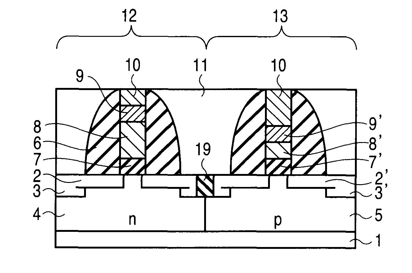
[0046]FIG. 1 is a sectional view of a semiconductor device according to a first embodiment of the present invention. An n-type semiconductor region 4 and a p-type semiconductor region 5 which are insulated from each other by a shallow trench isolation (STI) 19 are provided in a surface region of an Si substrate 1 as a semiconductor substrate. A p-channel MISFET 12 and an n-channel MISFET 13 are formed in the respective semiconductor regions. The n- and p-type semiconductor regions 4, 5 are formed as so-called wells.
[0047]A high-k gate insulating film (dielectric) 7 such as HfSiON is formed on the surface of the n-type semiconductor region 4. A gate insulating film 7′ is formed on the surface of the p-type semiconductor region 5, and this gate insulating film 7′ is based on a high-k gate insulating film such as HfSiON and contains at least one of groups IIA and IIIA metallic elements (e.g., Mg, Ca, Sr, Ba, Sc, Y, La, Ce, Pr, Nd, Pm, Sm, Eu, Gd, Tb, Dy, Ho, Er, Tm, Yb, Lu).
[0048]In ad...
second embodiment
[0077]FIG. 14 is a sectional view of a semiconductor device according to a second embodiment of the present invention. An n-type semiconductor region 4 and a p-type semiconductor region 5 are provided in a surface region of an Si substrate 1 as a semiconductor substrate. A p-channel MISFET 12 and an n-channel MISFET 13 are formed in the respective semiconductor regions. The n- and p-type semiconductor regions 4, 5 are formed as so-called wells.
[0078]A high-k gate insulating film 7 such as HfSiON is formed on the surface of the n-type semiconductor region 4. A gate insulating film 7′ is formed on the surface of the p-type semiconductor region 5, and this gate insulating film 7′ is based on a high-k gate insulating film such as HfSiON and contains at least one of groups IIA and IIIA metallic elements.
[0079]A lower gate electrode layer 14 based on, for example, TaCx is formed on the gate insulating film 7 located on the n-type semiconductor region. A lower gate electrode layer 8 based ...
second modification
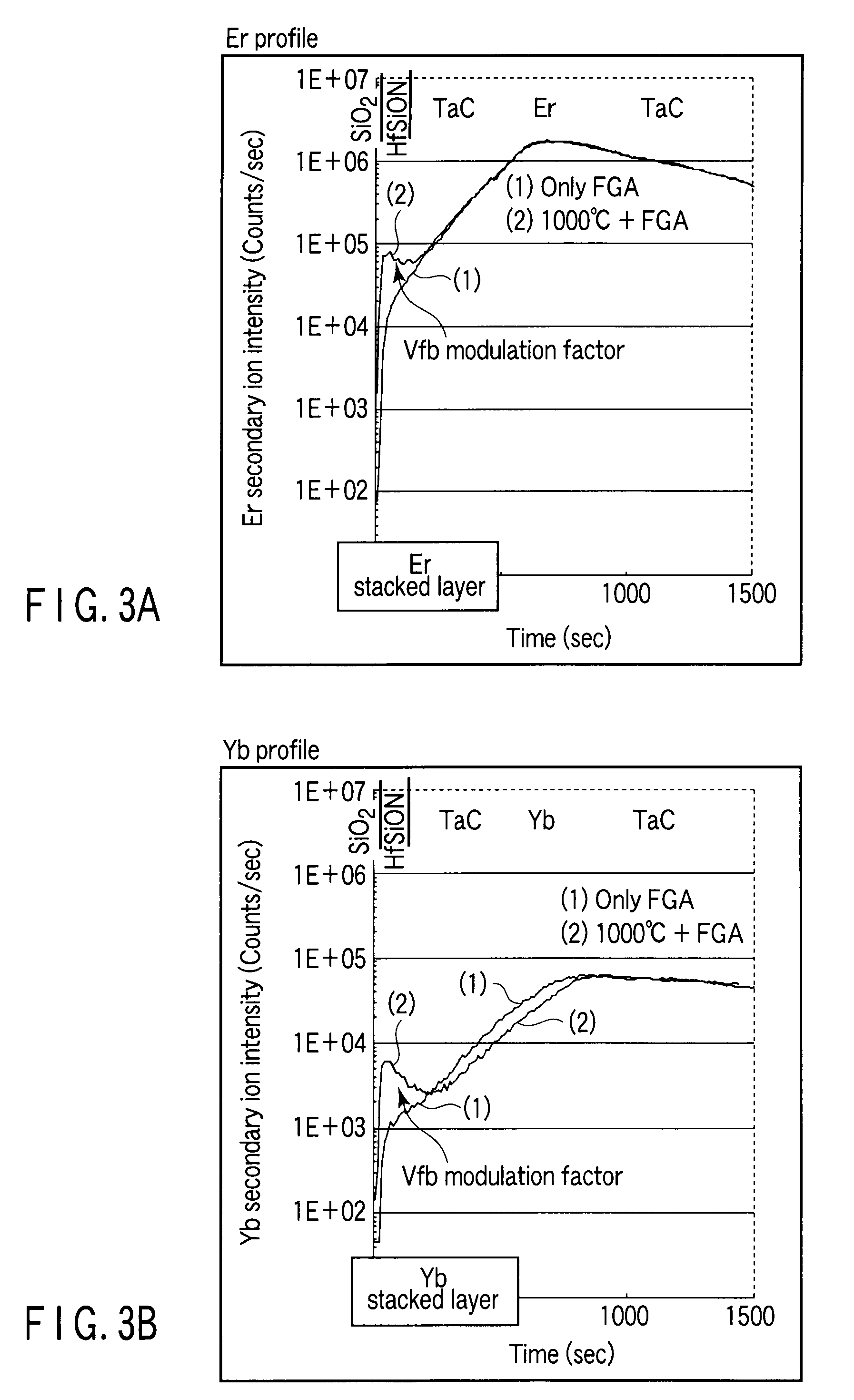
[0100]In the case described in the second embodiment, the high-density impurity diffusion layers are used as source / drain regions. It goes without saying that a so-called Schottky transistor which uses source / drain electrodes as the source / drain regions is also applicable.
[0101]Here, the heat treatment process for the source / drain electrodes is generally carried out at 600° C. or less. Therefore, it is desired that heat treatment be performed after the formation of a layer 9 and before the formation of the source / drain electrodes, and metallic elements diffused in a gate insulating film be used to reduce a threshold voltage. In addition, the temperature of this heat treatment is preferably 1000° C. or more. Moreover, a proper upper limit is 1100° C. or less which is the heat resistance temperature of a general gate insulating film / gate electrode.
[0102]According to the second embodiment, it is possible to provide a CMIS structure wherein the nonmetallic elements are simply implanted ...
PUM
 Abstract
Description
Claims
Application Information