Electrically non-interfering printing for electronic devices having capacitive touch sensors

a technology of capacitive touch and electronic devices, applied in the direction of electric/magnetic measurement arrangements, instruments, force measurement, etc., can solve the problems of electrical interference, compromise reliability, and interfering with the resulting electrical field

Active Publication Date: 2011-12-13
GOOGLE TECHNOLOGY HOLDINGS LLC
View PDF127 Cites 109 Cited by
  • Summary
  • Abstract
  • Description
  • Claims
  • Application Information

AI Technical Summary

Problems solved by technology

One problem associated with capacitive sensing technologies involves electrical interference.
Any material that interferes with this electrical field can compromise reliability.
For example, if the capacitive sensor is placed beneath a protective cover layer having vacuum-metalized printing, the metal in the printing can function as a shield, thereby interfering with the resulting electrical field and inhibiting the operation of the capacitive sensor.
This is a problem because device manufacturers often like to include printing somewhere on the surface of the device.
Without such printing, the user's ability to operate the device may be slowed or inhibited.

Method used


Image

  • Electrically non-interfering printing for electronic devices having capacitive touch sensors
  • Electrically non-interfering printing for electronic devices having capacitive touch sensors
  • Electrically non-interfering printing for electronic devices having capacitive touch sensors

Examples


Embodiment Construction

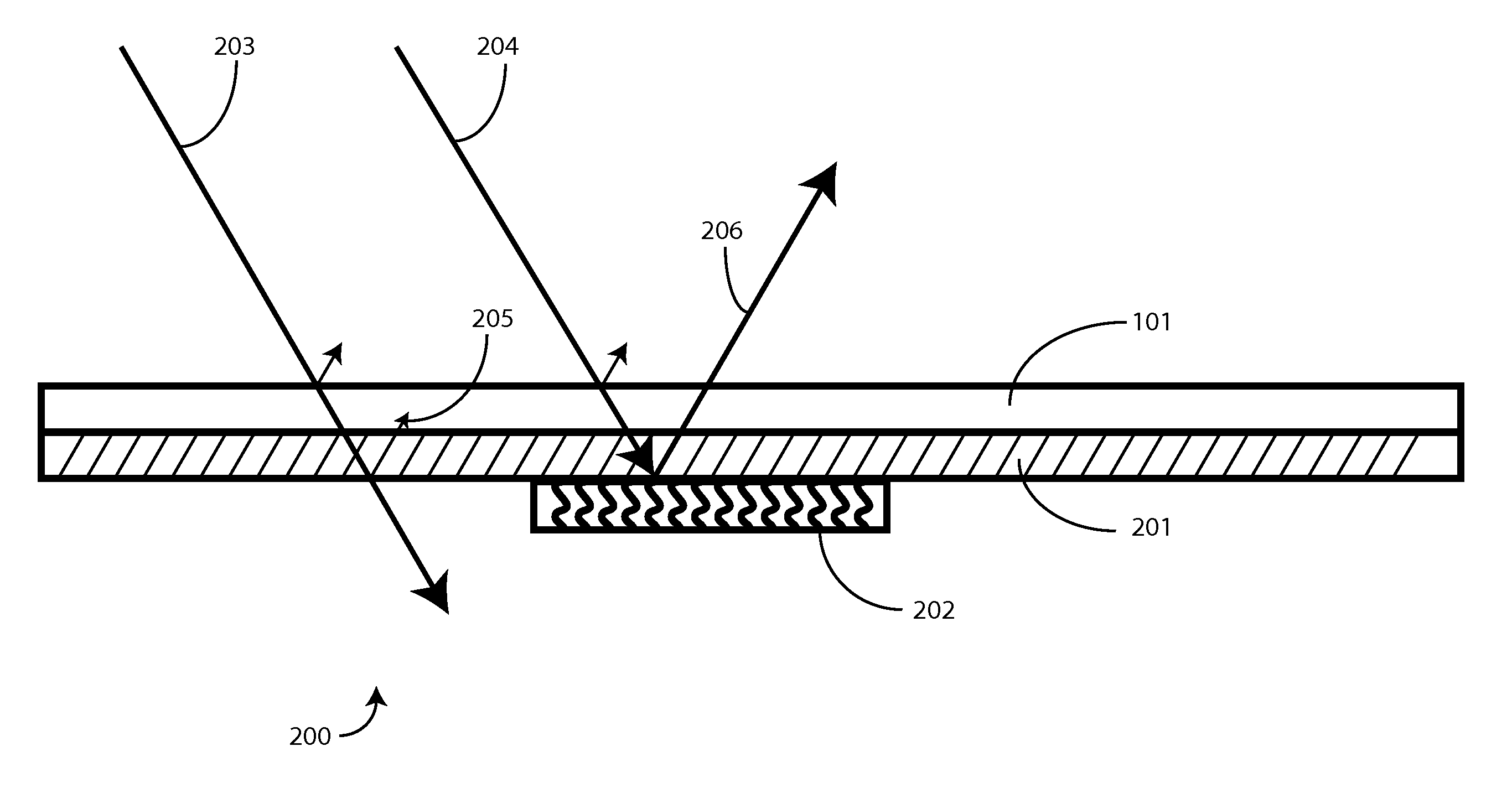
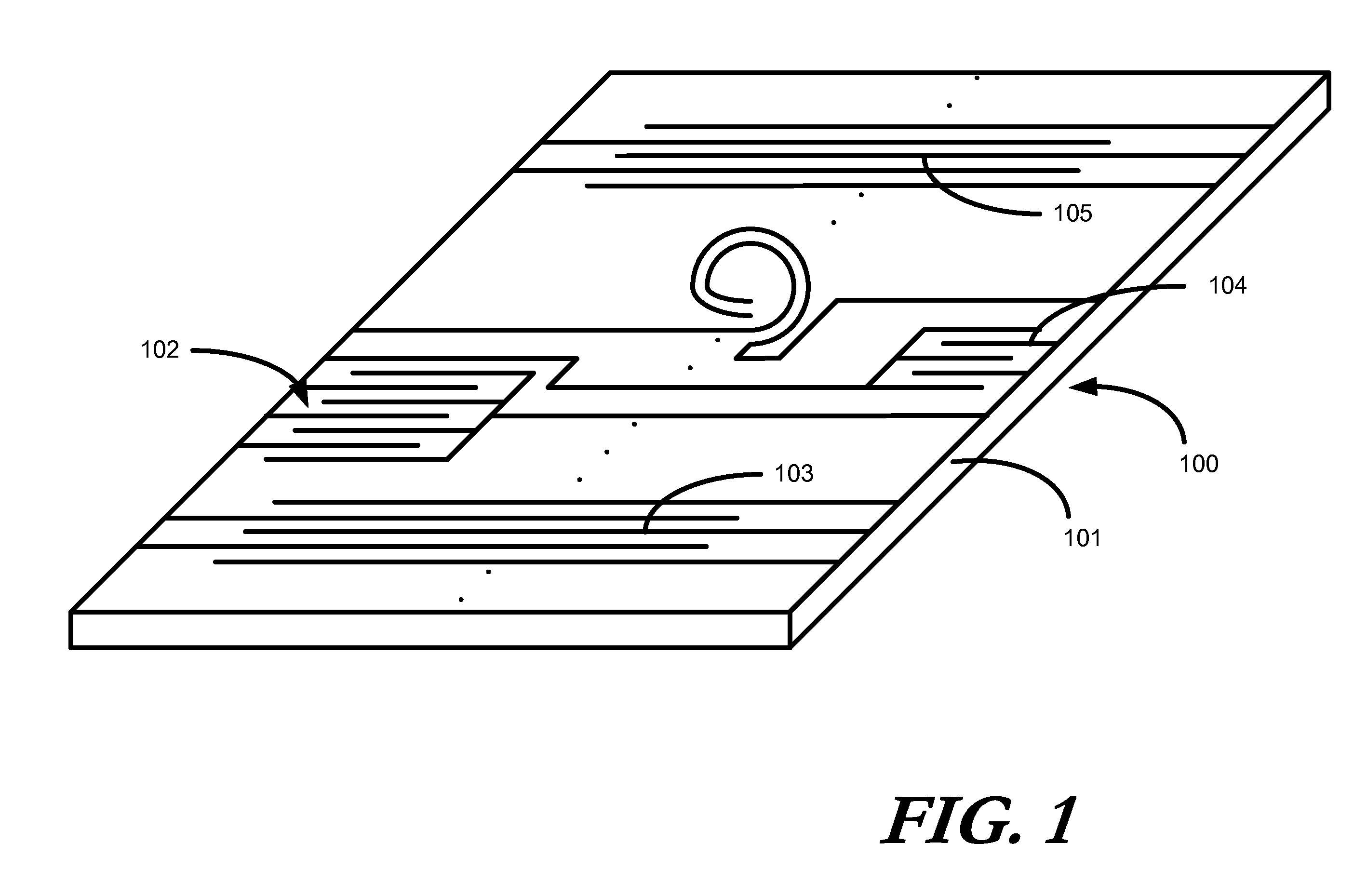
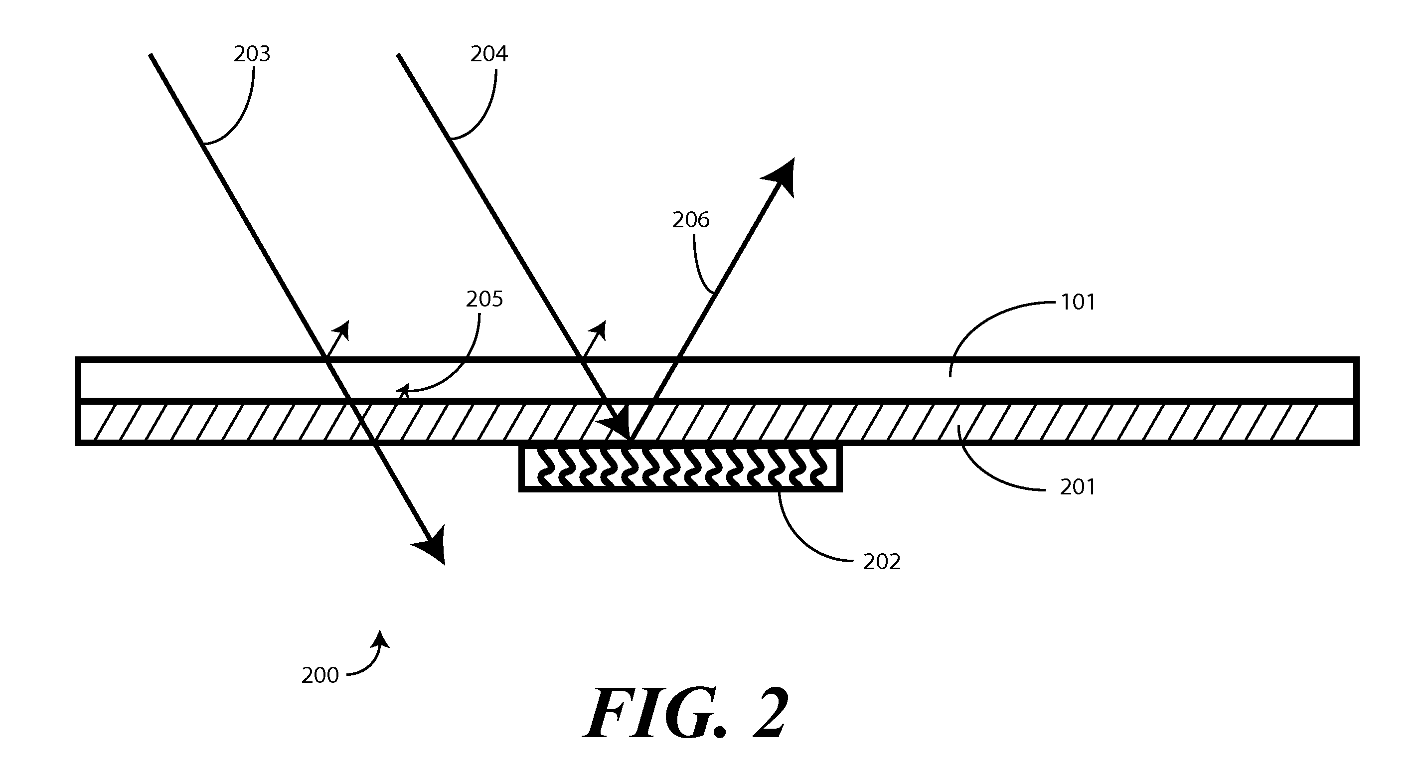
Before describing in detail embodiments that are in accordance with the present invention, it should be observed that the embodiments reside primarily in combinations of method steps and apparatus components related printing a non-electrically interfering graphic, visible to a user, for use in conjunction with a capacitive sensor or proximity detector. Accordingly, the apparatus components and method steps have been represented where appropriate by conventional symbols in the drawings, showing only those specific details that are pertinent to understanding the embodiments of the present invention so as not to obscure the disclosure with details that will be readily apparent to those of ordinary skill in the art having the benefit of the description herein.

Embodiments of the invention are now described in detail. Referring to the drawings, like numbers indicate like parts throughout the views. As used in the description herein and throughout the claims, the following terms take the m...


PUM


Abstract

A capacitive sensor (200) for a touch sensitive electronic device (800) includes at least one graphic (401) visible to a user. The graphic (401) is configured so as to be non-electrically interfering with the electrode array of the capacitive sensor (200). A substrate (101), configured to transmit light, has a layer of capacitive sensor material (201) deposited thereon. The layer of capacitive sensor material (201) is electrically conductive and pellucid. A layer of selectively disposed electrically conductive material (202) is then electrically coupled to the layer of capacitive sensor material (201). The layer of selectively disposed electrically conductive material (202) is arranged as a graphic, which may be a logo, brand, or other mark. The layer of selectively disposed electrically conductive material (202) has a reflectivity that is greater than the layer of capacitive sensor material (201) so as to make the graphic (401) visible to a user.

Description

BACKGROUND1. Technical FieldThis invention relates generally to capacitive sensors for electronic devices, and more specifically to a device having visible printing adjacent to capacitive sensing devices, where the visible printing does not interfere with the electrical operation of the sensing devices.2. Background ArtElectronic devices are continually becoming more advanced. The devices are becoming smaller, memories are becoming larger, more features are being added, and processing power is increasing. Some electronic devices today, including personal digital assistants and mobile telephones, have the processing power of a computer, yet still fit easily into a shirt pocket.One of the advances in electronic device technology involves the user interface. Traditional electronic devices generally included only keys or buttons for data entry. When a user wanted to enter a phone number, for example, the user pressed sequential buttons on the electronic device.The advent of the touch se...

Claims


Application Information

Patent Timeline
Patent Type & Authority Patents(United States)
IPC IPC(8): G06F3/041G01B7/16
CPCG06F3/044G06F3/0445G06F3/0447
Inventor EMIG, DAVID M.FOO, KEN K.
Owner GOOGLE TECHNOLOGY HOLDINGS LLC
Why Eureka
Try Eureka