Constructing variability maps by correlating off-state leakage emission images to layout information

a technology of layout information and leakage emission image, applied in image enhancement, semiconductor/solid-state device testing/measurement, instruments, etc., can solve the problems of low circuit performance and functional/parametric failure degrading manufacturing yield

Inactive Publication Date: 2012-03-06
IBM CORP
View PDF14 Cites 11 Cited by
  • Summary
  • Abstract
  • Description
  • Claims
  • Application Information

AI Technical Summary

Problems solved by technology

Increased process variations result in lower circuit performance and can potentially lead to functional / parametric failures degrading manufacturing yield.

Method used


Image

  • Constructing variability maps by correlating off-state leakage emission images to layout information
  • Constructing variability maps by correlating off-state leakage emission images to layout information
  • Constructing variability maps by correlating off-state leakage emission images to layout information

Examples


Embodiment Construction

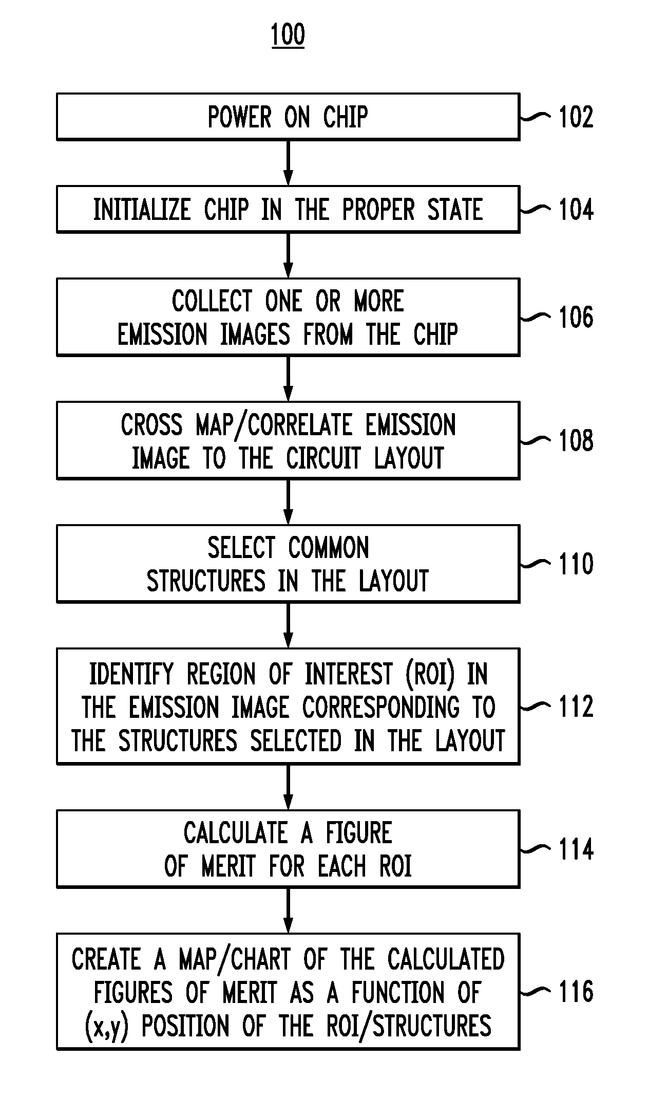
[0026]Illustrative embodiments of the invention will be described herein in the context of an illustrative integrated circuit testing environment. However, it is to be understood that principles of the invention are more generally applicable to a wide variety of other integrated circuit testing environments wherein it would be desirable to employ techniques for constructing chip variability maps quickly, easily, reliably and in a repeatable fashion.

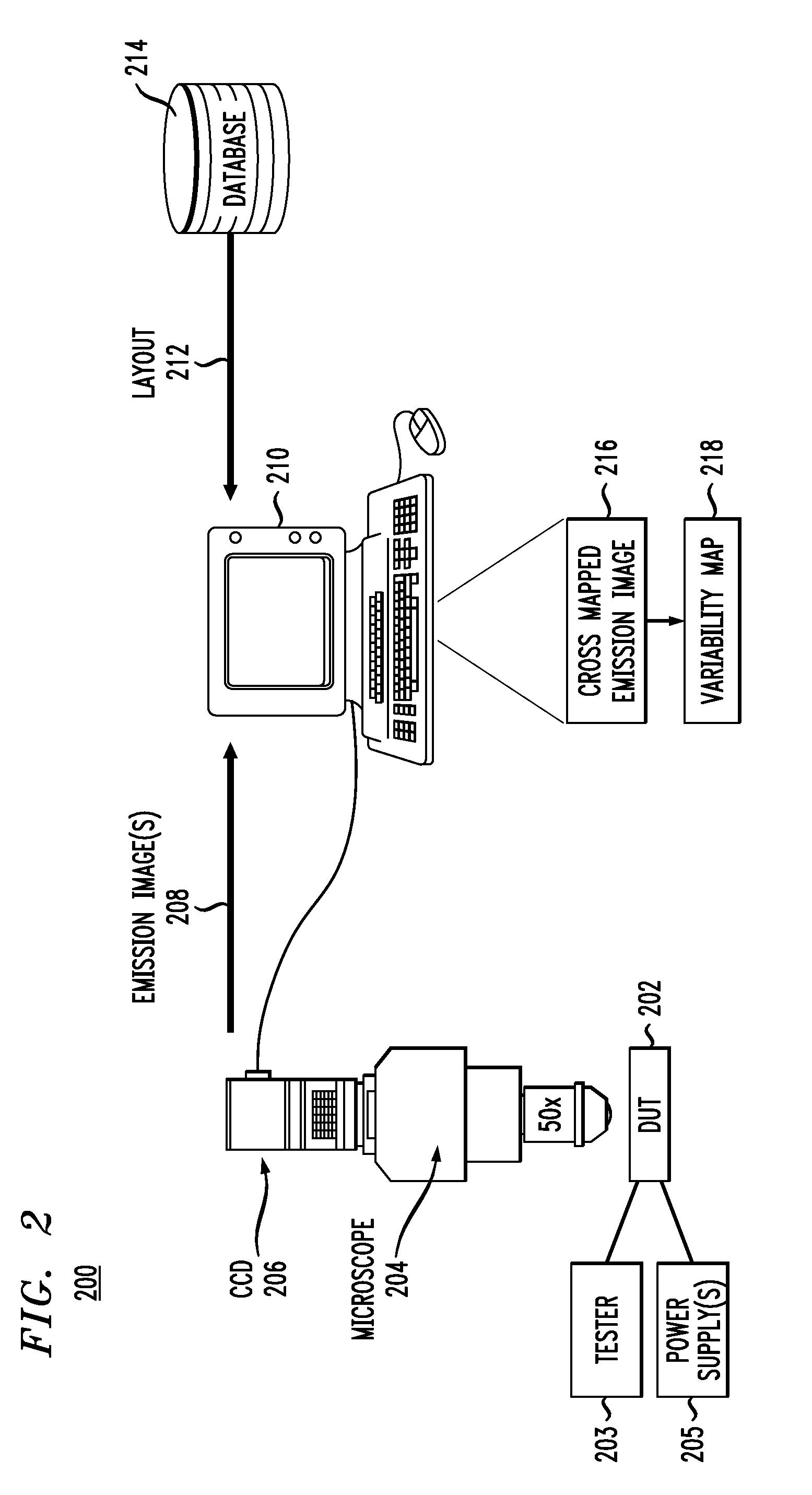
[0027]Such illustrative embodiments of the invention construct variability maps using images of energy being emitted in the near infrared spectrum by a device under test, such as an IC. The particular energy that is used in the illustrative embodiments is the Light Emission from Off-State Leakage Current (LEOSLC) from an IC.

[0028]It is noted that Polonsky et al. (see S. Polonsky, A. J. Weger, and M. K. McManus, U.S. Pat. No. 6,909,295, “Analysis methods of leakage current luminescence in CMOS circuits,” Jun. 21, 2005; and S. Polonsky, A. ...


PUM


Abstract

Improved techniques are disclosed for monitoring or sensing process variations in integrated circuit designs. Such techniques provide such improvements by constructing variability maps correlating leakage emission images to layout information. By way of example, a method for monitoring one or more manufacturing process variations associated with a device under test (e.g., integrated circuit) comprises the following steps. An emission image representing an energy emission associated with a leakage current of the device under test is obtained. The emission image is correlated with a layout of the device under test to form a cross emission image. Common structures on the cross emission image are selected and identified as regions of interest. One or more variability measures (e.g., figures of merit) are calculated based on the energy emissions associated with the regions of interest. A variability map is created based on the calculated variability measures, wherein the variability map is useable to monitor the one or more manufacturing process variations associated with the device under test.

Description

FIELD OF THE INVENTION[0001]The present invention generally relates to integrated circuit designs and, more particularly, to improved techniques for monitoring or sensing process variations in such integrated circuit designs.BACKGROUND OF THE INVENTION[0002]The ever increasing need for high performance and increased chip (integrated circuit or IC) functionality with lower costs has resulted in aggressive scaling of transistor dimensions. As transistor dimensions are scaled down, the effect of parameter variations on circuit robustness increases. Increased process variations result in lower circuit performance and can potentially lead to functional / parametric failures degrading manufacturing yield.[0003]Process variations can be classified into distinct categories: process variations can be “inter-die” or “intra-die;” and process variations can also be “random” or “systematic.” An inter-die process variation is a process variation across multiple dies. An intra-die process variation ...

Claims


Application Information

Patent Timeline
Patent Type & Authority Patents(United States)
IPC IPC(8): G06K9/00
CPCG06T7/001G06T2207/30148G01R31/26H01L22/00
Inventor POLONSKY, STANISLAVSONG, PEILINSTELLARI, FRANCOWEGER, ALAN J.
Owner IBM CORP
Why Eureka
Try Eureka