Semiconductor integrated circuit, semiconductor integrated circuit control method, and terminal system
a technology of semiconductor integrated circuits and integrated circuits, applied in the direction of generating/distributing signals, pulse techniques, instruments, etc., can solve the problem that the power cutoff technique cannot apply the technology for suppressing the clock skew described above, and achieve the effect of reducing the clock skew between the logic blocks and reducing the clock skew
- Summary
- Abstract
- Description
- Claims
- Application Information
AI Technical Summary
Benefits of technology
Problems solved by technology
Method used
Image

Examples
first embodiment
[0062]The following describes a first embodiment of the present invention, with reference to the drawings.
[0063]
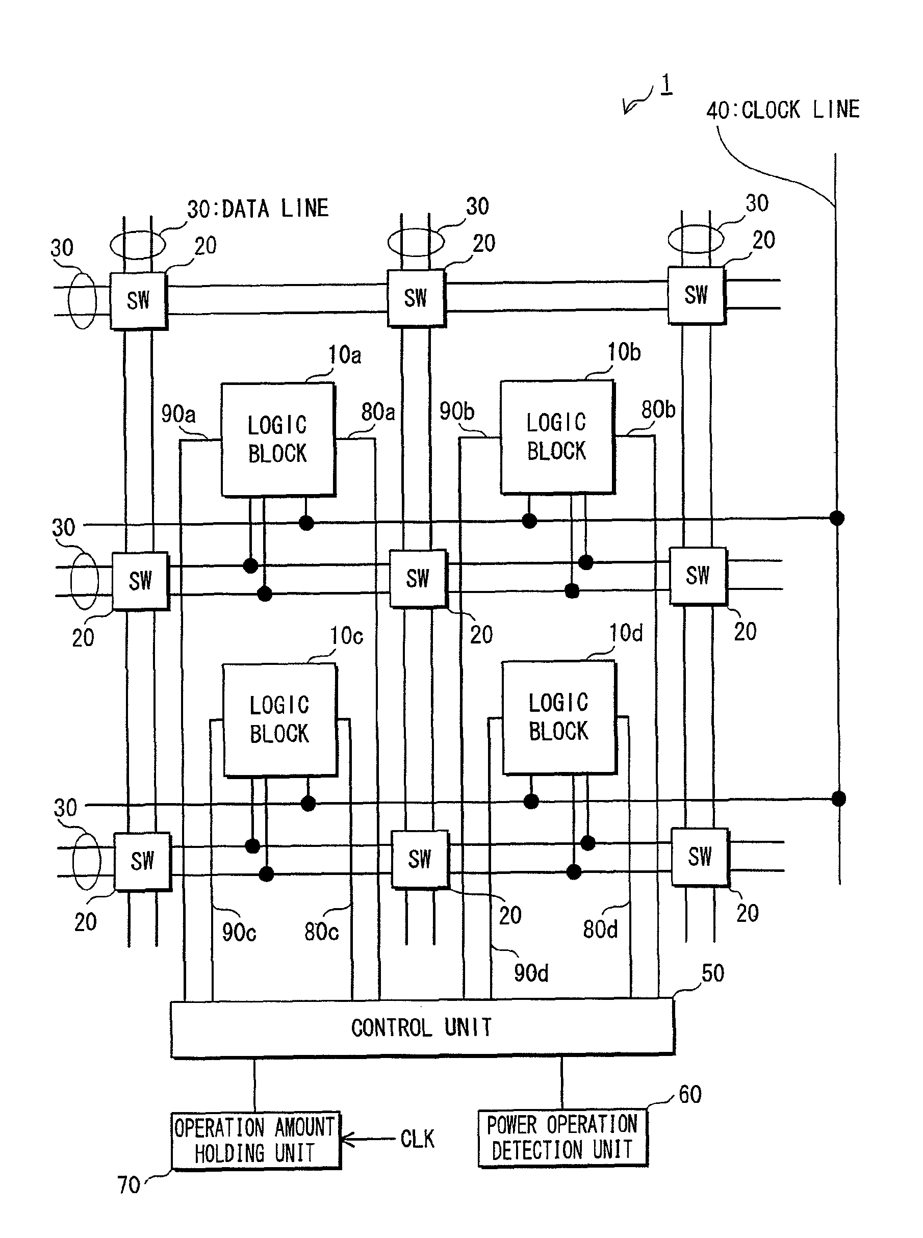
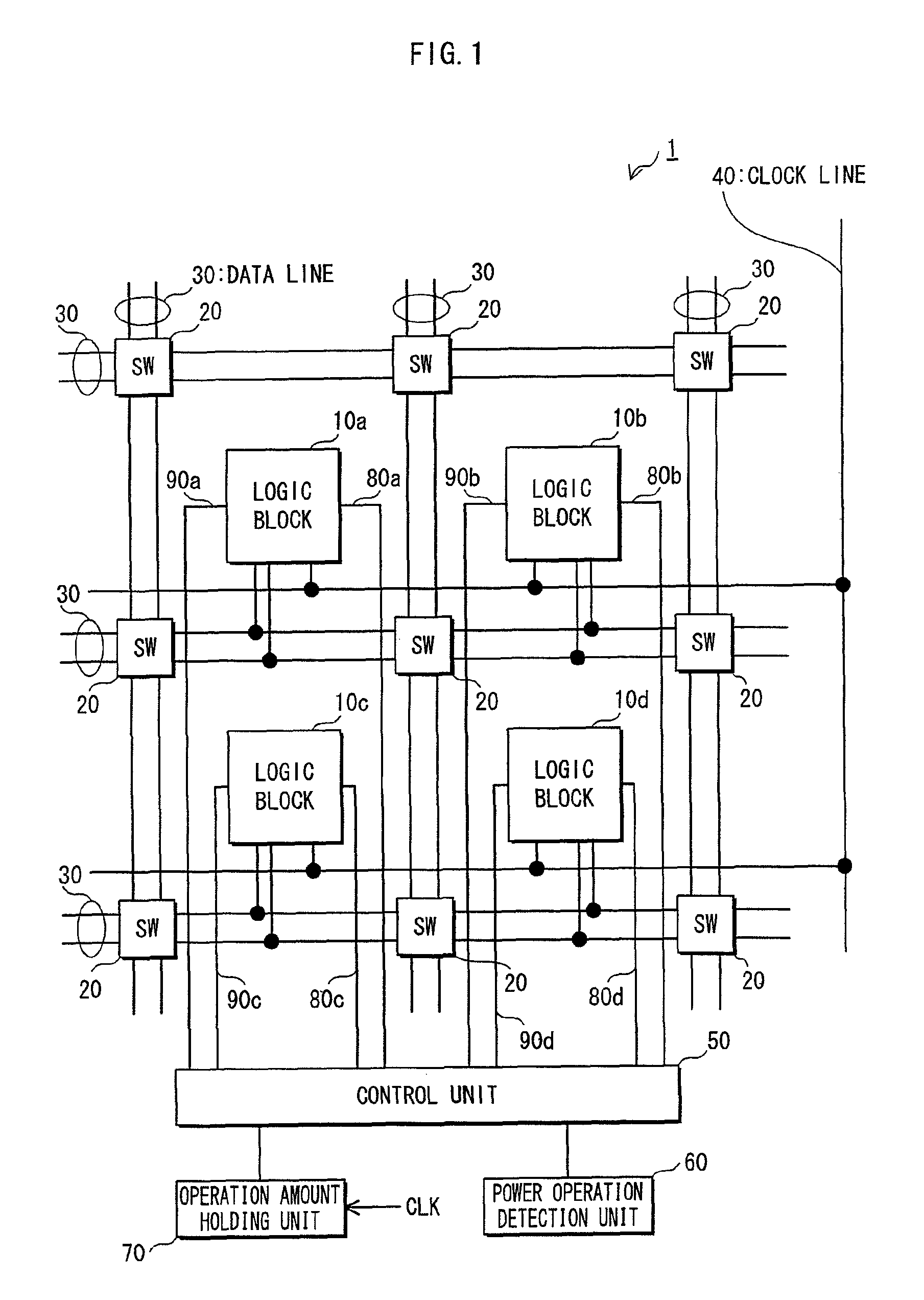
[0064]The following describes the configuration of a semiconductor circuit according to the present embodiment, with reference to FIG. 1. FIG. 1 shows the configuration of the semiconductor integrated circuit according to the present embodiment. Here, the semiconductor integrated circuit may be a programmable logic circuit whose functions are changeable by a program such as an FPGA (Field Programmable Gate Array), reconfigurable logic, or the like.
[0065]In FIG. 1, a semiconductor integrated circuit 1 includes logic blocks 10a to 10d, a data line 30, and a line selector 20. The data line 30 is for transmitting and receiving data between each of the logic blocks 10a to 10d, and the line selector 20 is for changing the setting of the connection state of the data line 30 between each of the logic blocks 10a to 10d, depending on a program.
[0066]The semiconductor integrated circ...
specific example
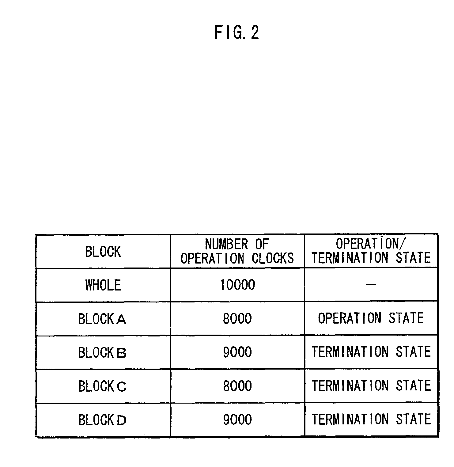
[0113]The following describes, with reference to FIGS. 8A and 8B, a specific example of the operation of the semiconductor integrated circuit 1 that has been described with references FIGS. 1 to 7. FIGS. 8A and 8B are each a diagram for explaining a specific example of the logic block control process performed by the semiconductor integrated circuit shown in FIG. 1.
[0114]In this specific example, the semiconductor integrated circuit 1 performs operations in order of configurations A, B, C, and D, where in configuration A, logic blocks that need to be operated for the execution of a target process are the logic blocks 10a to 10d; in configuration B, a logic block that needs to be in operation is only the logic block 10a; in configuration C, logic blocks that need to be in operation are 10a to 10d; and in configuration D, a logic block that needs to be in operation is the logic block 10c.
[0115]It is assumed that the power unit performs the discharge operation while the semiconductor ...
second embodiment
[0122]The following describes the second embodiment of the present invention, with reference to the drawings.
[0123]Note that, while a gated clock technique is used in the first embodiment, a power cutoff technique is used in the present embodiment. Here, the gated clock technique is for stopping the supply of clocks so as to terminate the operation of the logic blocks, and the power cutoff technique is for stopping the power so as to terminate the operation of the logic blocks.
[0124]In the second embodiment, descriptions of components that are substantially the same as the components of the first embodiment are omitted, since the same descriptions as those used in the first embodiment are applicable with use of the same reference numbers as those used in the first embodiment.
[0125]
[0126]The following describes the configuration of a semiconductor integrated circuit of the present embodiment, with reference to FIG. 9. FIG. 9 shows the configuration of the semiconductor integrated cir...
PUM
 Abstract
Description
Claims
Application Information
 - R&D
- Intellectual Property
- Life Sciences
- Materials
- Tech Scout
- Unparalleled Data Quality
- Higher Quality Content
- 60% Fewer Hallucinations
Browse by: Latest US Patents, China's latest patents, Technical Efficacy Thesaurus, Application Domain, Technology Topic, Popular Technical Reports.
© 2025 PatSnap. All rights reserved.Legal|Privacy policy|Modern Slavery Act Transparency Statement|Sitemap|About US| Contact US: help@patsnap.com