Check patentability & draft patents in minutes with Patsnap Eureka AI!

Semiconductor integrated circuit, semiconductor integrated circuit control method, and terminal system

a technology of semiconductor integrated circuits and integrated circuits, applied in the direction of generating/distributing signals, pulse techniques, instruments, etc., can solve the problems of reducing the clock skew between logic blocks, affecting the clock skew, and failing to operate properly

Inactive Publication Date: 2009-11-05
PANASONIC CORP
View PDF6 Cites 1 Cited by
  • Summary
  • Abstract
  • Description
  • Claims
  • Application Information

AI Technical Summary

Benefits of technology

[0015]According to each of the semiconductor integrated circuit, the method for controlling the same, and the terminal system, the logic blocks are controlled such that each of the logic blocks enter a corresponding one of states which include an operation state and a termination state, depending on the past state of each logic block, while the power unit that supplies power to the semiconductor integrated circuit is performing an operation in which power saving is unnecessary. Here, the operation state is a state in which the logic blocks are in operation, and the termination state is a state in which the logic blocks are not in operation. Therefore, a difference of the deterioration degree is small between the logic blocks during a period in which power saving is unnecessary, resulting in the clock skew between the logic blocks being reduced.
[0016]In the above-described semiconductor integrated circuit, the predetermined operation may be a charge operation of the power unit.
[0017]When the power unit is in the charge operation, power may be supplied from, for example, a commercial power source. Therefore, the clock skew is reduced during the period in which power saving is unnecessary in terms of the operation time.
[0018]In the above-described semiconductor integrated circuit, when the operation information indicates a discharge operation of the power unit in which power saving is necessary, the state determination unit may further determine a state of each logic block that needs to be operated for an execution of a target process, as an operation state in which each logic block is in operation.
[0019]When the power unit is performing the discharge operation, the semiconductor integrated circuit preferably performs an operation in which power saving is necessary in terms of the operation time.
[0020]The stated structure meets the above-described demand, since only a logic block that needs to be operated for the execution of a target process by the semiconductor integrated circuit is operated, when the power unit is performing the discharge operation.

Problems solved by technology

When more than a predetermined amount of the clock skew occurs, an error occurs, for example, in the transmission and reception of data between the registers, resulting in the LSI failing to operate properly.
However, transistors included in the LSI, especially a P-channel MOS transistor, deteriorate over time due to NBTI (Negative Bias Temperature Instability), HCI (Hot Carrier Injection) and such.
A difference in deterioration degree is a cause for the occurrence of the clock skew.
However, the deterioration of transistors over time is not taken into consideration in the above-described technique.
Therefore, with the above-described technique, it is impossible to prevent the operation failure of LSIs due to the clock skew that is caused by the deterioration of transistors over time.

Method used


Image

  • Semiconductor integrated circuit, semiconductor integrated circuit control method, and terminal system
  • Semiconductor integrated circuit, semiconductor integrated circuit control method, and terminal system
  • Semiconductor integrated circuit, semiconductor integrated circuit control method, and terminal system

Examples


first embodiment

[0060]The following describes a first embodiment of the present invention, with reference to the drawings.

[0061]

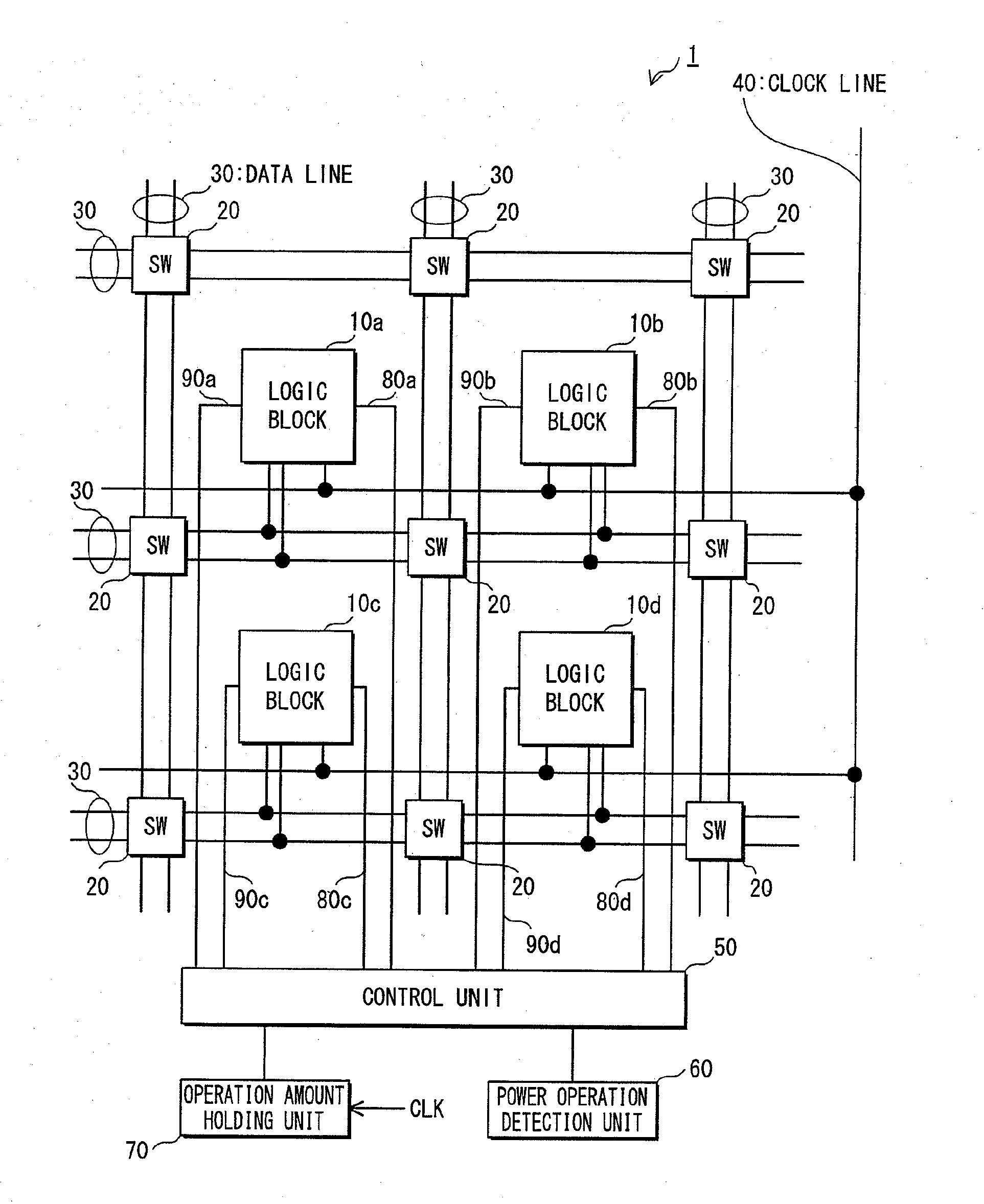
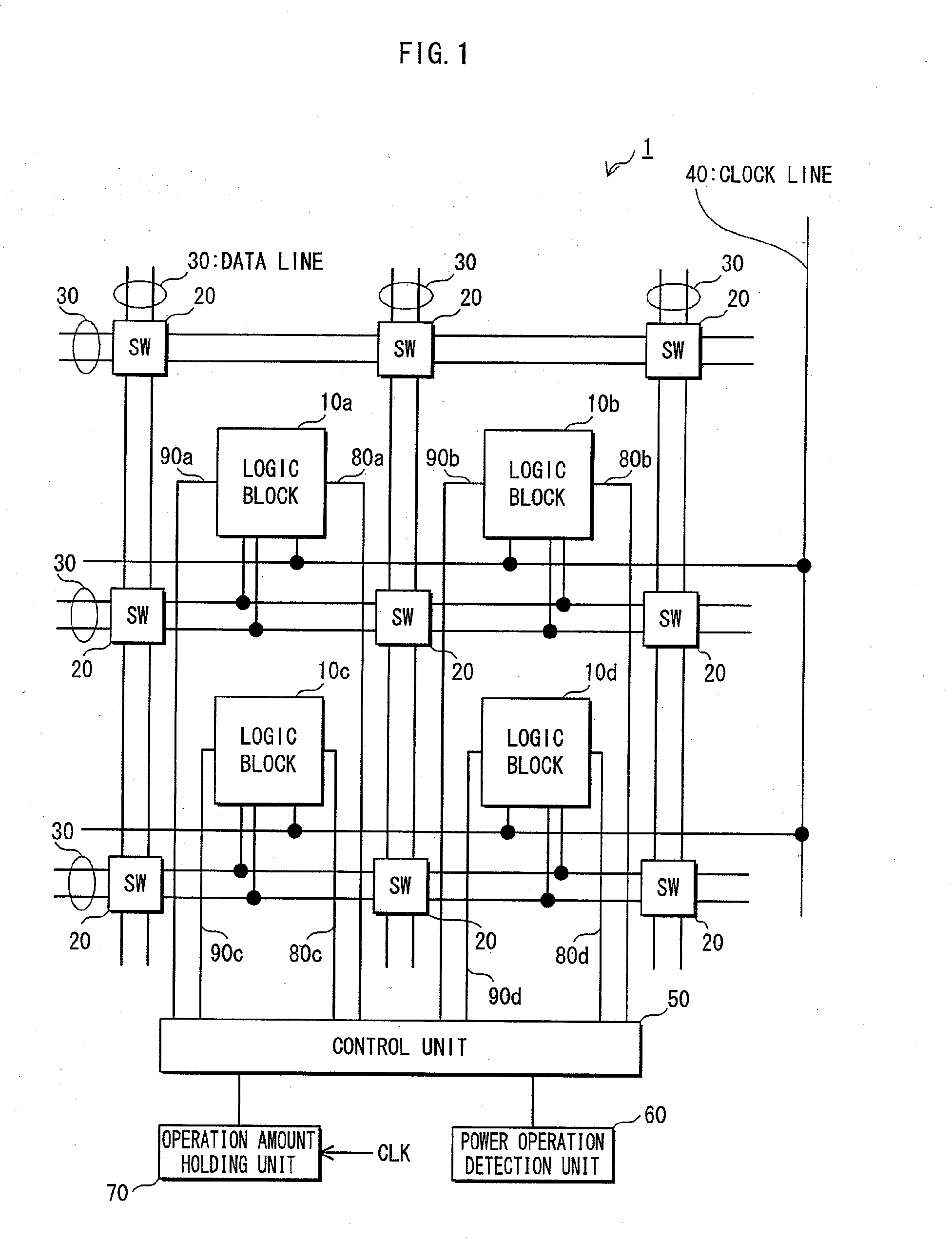
[0062]The following describes the configuration of a semiconductor circuit according to the present embodiment, with reference to FIG. 1. FIG. 1 shows the configuration of the semiconductor integrated circuit according to the present embodiment. Here, the semiconductor integrated circuit may be a programmable logic circuit whose functions are changeable by a program such as an FPGA (Field Programmable Gate Array), reconfigurable logic, or the like.

[0063]In FIG. 1, a semiconductor integrated circuit 1 includes logic blocks 10a to 10d, a data line 30, and a line selector 20. The data line 30 is for transmitting and receiving data between each of the logic blocks 10a to 10d, and the line selector 20 is for changing the setting of the connection state of the data line 30 between each of the logic blocks 10a to 10d, depending on a program.

[0064]The semiconductor integrated circ...

specific example

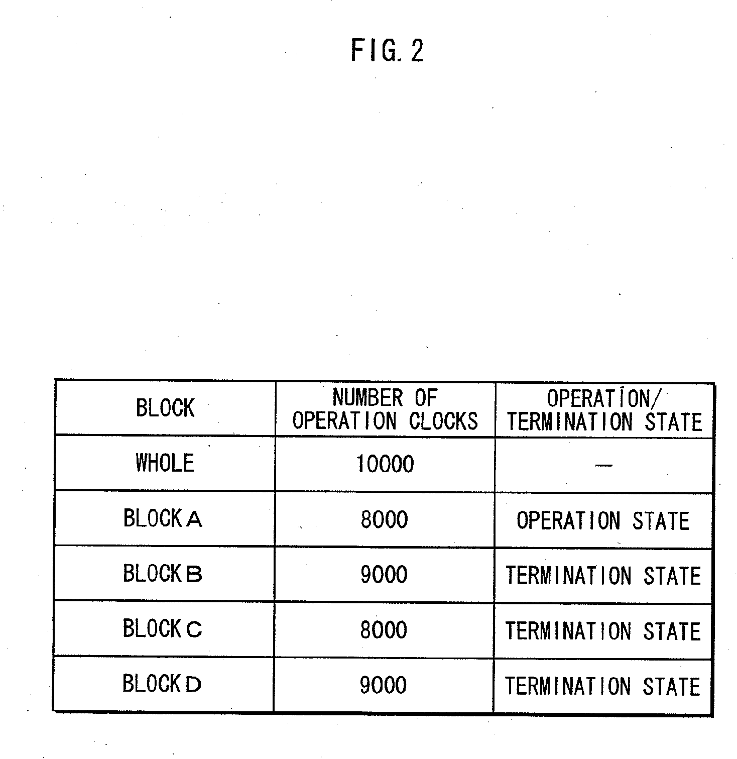
[0111]The following describes, with reference to FIGS. 8A and 8B, a specific example of the operation of the semiconductor integrated circuit 1 that has been described with references FIGS. 1 to 7. FIGS. 8A and 8B are each a diagram for explaining a specific example of the logic block control process performed by the semiconductor integrated circuit shown in FIG. 1.

[0112]In this specific example, the semiconductor integrated circuit 1 performs operations in order of configurations A, B, C, and D, where in configuration A, logic blocks that need to be operated for the execution of a target process are the logic blocks 10a to 10d; in configuration B, a logic block that needs to be in operation is only the logic block 10a; in configuration C, logic blocks that need to be in operation are 10a to 10d; and in configuration D, a logic block that needs to be in operation is the logic block 10c.

[0113]It is assumed that the power unit performs the discharge operation while the semiconductor ...

second embodiment

[0120]The following describes the second embodiment of the present invention, with reference to the drawings.

[0121]Note that, while a gated clock technique is used in the first embodiment, a power cutoff technique is used in the present embodiment. Here, the gated clock technique is for stopping the supply of clocks so as to terminate the operation of the logic blocks, and the power cutoff technique is for stopping the power so as to terminate the operation of the logic blocks.

[0122]In the second embodiment, descriptions of components that are substantially the same as the components of the first embodiment are omitted, since the same descriptions as those used in the first embodiment are applicable with use of the same reference numbers as those used in the first embodiment.

[0123]

[0124]The following describes the configuration of a semiconductor integrated circuit of the present embodiment, with reference to FIG. 9. FIG. 9 shows the configuration of the semiconductor integrated cir...


PUM


Abstract

A semiconductor integrated circuit 1 judges whether a power unit is performing a discharge operation or a charge operation. To reduce clock skew between a plurality of logic blocks in the semiconductor integrated circuit 1, when the power unit is performing the charge operation, the semiconductor integrated circuit 1 determines a logic block that needs to be operated for the execution of a target process, as an operation block whose operation is to be started, and, determines, in the rest of the logic blocks, a logic block having a termination rate whose value is larger than a value of the minimum termination rate, as the operation block whose operation is to be started, the value of the termination rate being larger by more than a predetermined value.

Description

TECHNICAL FIELD[0001]The present invention relates to a technique for preventing an increase of clock skew caused by the deterioration of a plurality of logic blocks over time.BACKGROUND ART[0002]In a synchronous design method that has been popularly used in an LSI (Large Scale Integration) design in recent years, a clock signal for control is supplied to, for example, state registers, at the same timing. In an actual LSI, the amount of delay of the clock signal caused between a clock generation source and a register is different between each of the registers, depending on a difference in the configuration of a clock supply circuit. Note that the difference of the amount of delay between devices such as the registers is referred to as clock skew.[0003]When more than a predetermined amount of the clock skew occurs, an error occurs, for example, in the transmission and reception of data between the registers, resulting in the LSI failing to operate properly. Therefore, in general, whe...

Claims


Application Information

Patent Timeline
Patent Type & Authority Applications(United States)
IPC IPC(8): H03K19/173H03K19/0175
CPCG06F1/10H03K19/17784H03K19/1774H03K5/1502
Inventor ICHINOMIYA, TAKAHIRO
Owner PANASONIC CORP
Features
  • R&D
  • Intellectual Property
  • Life Sciences
  • Materials
  • Tech Scout
  • Unparalleled Data Quality
  • Higher Quality Content
  • 60% Fewer Hallucinations
Learn More