GaN-based semiconductor light-emitting device, light illuminator, image display planar light source device, and liquid crystal display assembly

a semiconductor and light-emitting technology, applied in semiconductor lasers, instruments, optics, etc., can solve the problems of shifting the emission wavelength, narrowing the color space after control, and reducing the efficiency of the light-emitting device, so as to reduce the emission wavelength shift, control the luminance in a wider range, and increase the operating current density

Active Publication Date: 2012-05-01
SONY SEMICON SOLUTIONS CORP
View PDF48 Cites 10 Cited by
  • Summary
  • Abstract
  • Description
  • Claims
  • Application Information

AI Technical Summary

Benefits of technology

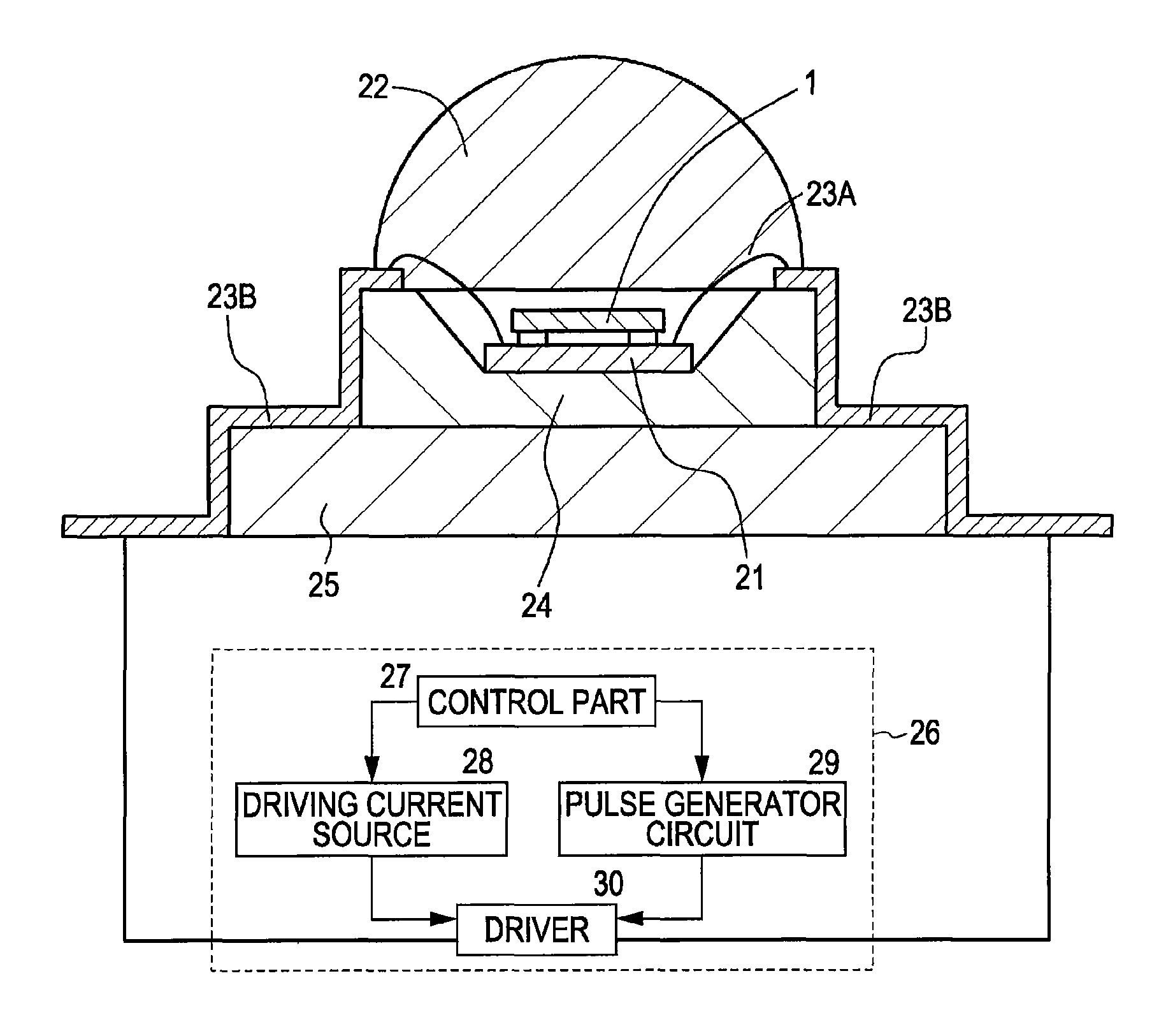
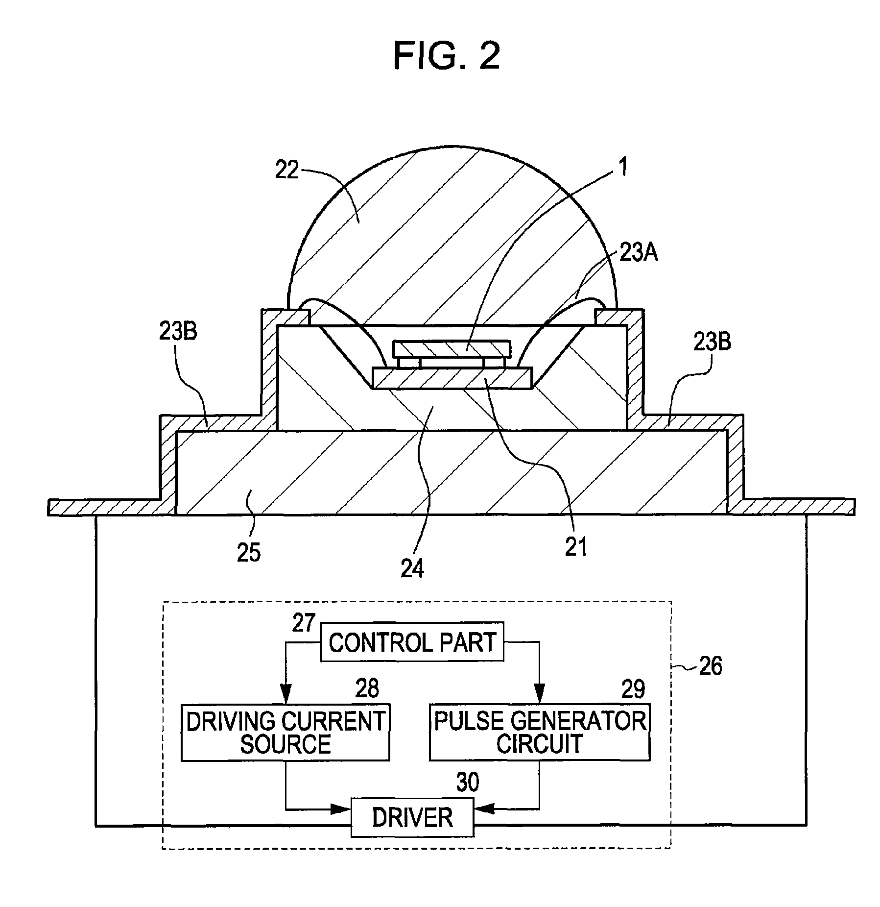
[0024]Therefore, an object of the present invention is to provide a GaN-based semiconductor light-emitting device having a structure capable of suppressing a large shift of the emission wavelength due to an increase in operating current density and capable of controlling luminance in a wider range, and a light illuminator, an image display, a planar light source device, and a liquid crystal display assembly in each of which the GaN-based semiconductor light-emitting device is incorporated.

Problems solved by technology

Such an emission wavelength shift due to an increase in the driving current (operating current) is a problem common to active layers composed of GaN-based compound semiconductors containing In atoms which have a visible wavelength or longer wavelength.
However, as described above, the use of such means causes the problem of shifting the emission wavelength due to an increase in the driving current (operating current).
However, as described above, when the emission wavelength of each light-emitting device is shifted to an emission wavelength different from a desired emission wavelength, there is the problem of narrowing the color space after control.
However, in this liquid crystal display, when the driving current (operating current) of the GaN-based semiconductor light-emitting device is increased for increasing the luminance (brightness) of the back light, a shift of the emission wavelength of the GaN-based semiconductor light-emitting device may cause the problem of narrowing or changing the color space.
However, in this case, with the same operating current, the operating current density is increased, thereby resulting in the problem of shifting the emission wavelength at a high operating current density.
Furthermore, the above-described patent application publications or documents do not disclose a technique for suppressing a large shift of the emission wavelength due to an increase in operating current density.
Therefore, it is difficult to directly compare current dependencies of characteristics.
However, in a GaN-based semiconductor light-emitting device of a smaller size, the effect of decreasing a shift of the emission wavelength is significant.
In addition, with respect to the carrier transmittance of a hetero-barrier including a well layer and a barrier layer, another possible cause is that holes with large effective mass have difficulty in reaching a well layer on the first GaN-based compound semiconductor layer side through a plurality of barrier layers.

Method used


Image

  • GaN-based semiconductor light-emitting device, light illuminator, image display planar light source device, and liquid crystal display assembly
  • GaN-based semiconductor light-emitting device, light illuminator, image display planar light source device, and liquid crystal display assembly
  • GaN-based semiconductor light-emitting device, light illuminator, image display planar light source device, and liquid crystal display assembly

Examples


example 1

EQUIVALENT

[0249]d2=(WL2 / WL) / (t2 / t0)=(8 / 10) / (50 / 150)=2.40d1=(WL1 / WL) / (t1 / t0)=(2 / 10) / (100 / 150)=0.30

example 2

[0266]Example 2 is a modification of Example 1. In a GaN-based semiconductor light-emitting device of Example 2, an underlying layer containing In atoms is formed between the first GaN-based compound semiconductor layer 13 and the active layer 15 (more specifically, the first GaN-based compound semiconductor layer 13 and the undoped GaN layer 14 in Example 2). In addition, a superlattice layer containing a p-type dopant is formed between the active layer 15 and the second GaN-based compound semiconductor layer 17 (more specifically, the undoped GaN layer 16 and the second GaN-based compound semiconductor layer 17 in Example 2). In this structure, a more stable operation of the GaN-based semiconductor light-emitting device can be achieved at a high operating current density while further improving the luminous efficiency and further decreasing the operating voltage.

[0267]The underlying layer is a Si-doped InGaN layer having an In composition ratio of 0.03 and a thickness of 150 nm. T...

example 3

[0272]d2=(WL2 / WL) / (t2 / t0)={(5+2 / 9) / 10} / {(40+2 / 3) / 122}=1.57d1=(WL1 / WL) / (t1 / t0)={(4+7 / 9) / 10} / {(81+1 / 3) / 122}=0.72

[0273]For comparison, a GaN-based semiconductor light-emitting device including an active layer shown as Comparative Example 3 in Table 3 was produced. The well layer density d1 and the well layer density d2 in Comparative Example 3 are determined from the equations (1-1) and (1-2) as follows:


PUM


Abstract

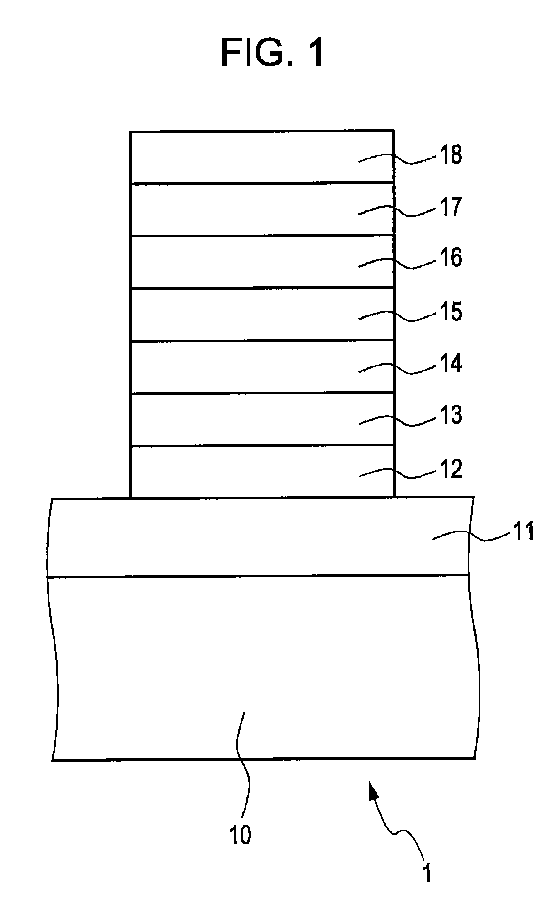
A GaN-based semiconductor light-emitting device includes (A) a first GaN-based compound semiconductor layer 13 having n-type conductivity, (B) an active layer 15 having a multi-quantum well structure including well layers and barrier layers for separating between the well layers, and (C) a second GaN-based compound semiconductor layer 17 having p-type conductivity. The well layers are disposed in the active layer 15 so as to satisfy the relation d1<d2 wherein d1 is the well layer density on the first GaN-based compound semiconductor layer side in the active layer and d2 is the well layer density on the second GaN-based compound semiconductor layer side.

Description

CROSS REFERENCE TO RELATED APPLICATIONS[0001]The present application claims priority to Japanese Patent Document Nos. 2005-264938 filed on Sep. 13, 2005, and 2006-234199 filed on Aug. 30, 2006, the disclosures of which are herein incorporated by reference.BACKGROUND[0002]The present invention relates to a GaN-based semiconductor light-emitting device and a light illuminator, an image display, a planar light source device, and a liquid crystal display assembly in each of which the GaN-based semiconductor light-emitting device is incorporated.BACKGROUND ART[0003]In a light-emitting device (GaN-based semiconductor light-emitting device) including an active layer composed of a gallium nitride (GaN)-based compound semiconductor, the band-gap energy can be controlled by changing the alloy composition or thickness of the active layer to realize emission wavelengths in a wide range from ultraviolet to infrared. GaN-based semiconductor light-emitting devices emitting various color lights hav...

Claims


Application Information

Patent Timeline
Patent Type & Authority Patents(United States)
IPC IPC(8): H01L29/15H01L33/06H01L33/08H01L33/20H01L33/32H01L33/40H01L33/58
CPCB82Y20/00H01L33/06H01L33/32G02F1/133603G02F1/133621H01S5/3086H01S5/309H01S5/34333H01L33/20H04N9/315H01L2224/16145H01L2224/48091H01L2224/48247H01L2224/45144H01L2224/0603H01L2224/48137H01L2924/181H01L2924/13091H01L2924/00014H01L2924/00012H01L2924/00
Inventor BIWA, GOSHIOKUYAMA, HIROYUKI
Owner SONY SEMICON SOLUTIONS CORP
Why Eureka
Try Eureka