

Layouts for the monolithic integration of CMOS and deposited photonic active layers
a technology of photonic active layers and monolithic integration, which is applied in the direction of material analysis, radio frequency controlled devices, instruments, etc., can solve the problems of low “charge-to-voltage” conversion efficiency, circuitry that cannot allow the aggregation of signals, and cannot be bandgap engineered
- Summary
- Abstract
- Description
- Claims
- Application Information
AI Technical Summary
Benefits of technology
Problems solved by technology
Method used
Image

Examples
Embodiment Construction
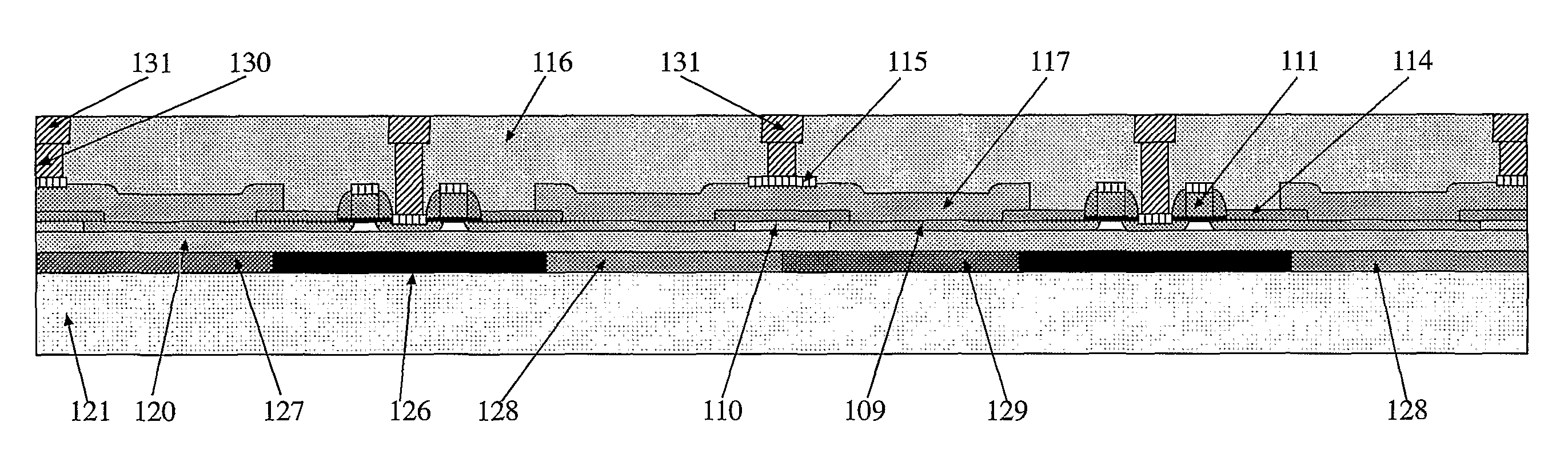
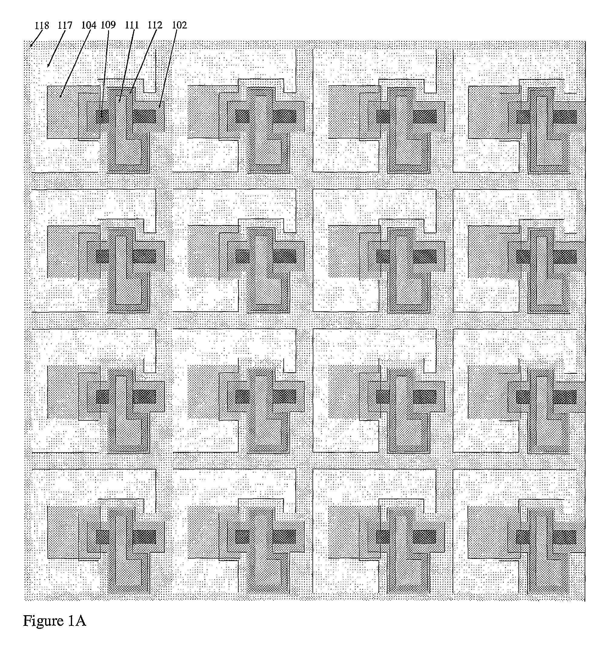
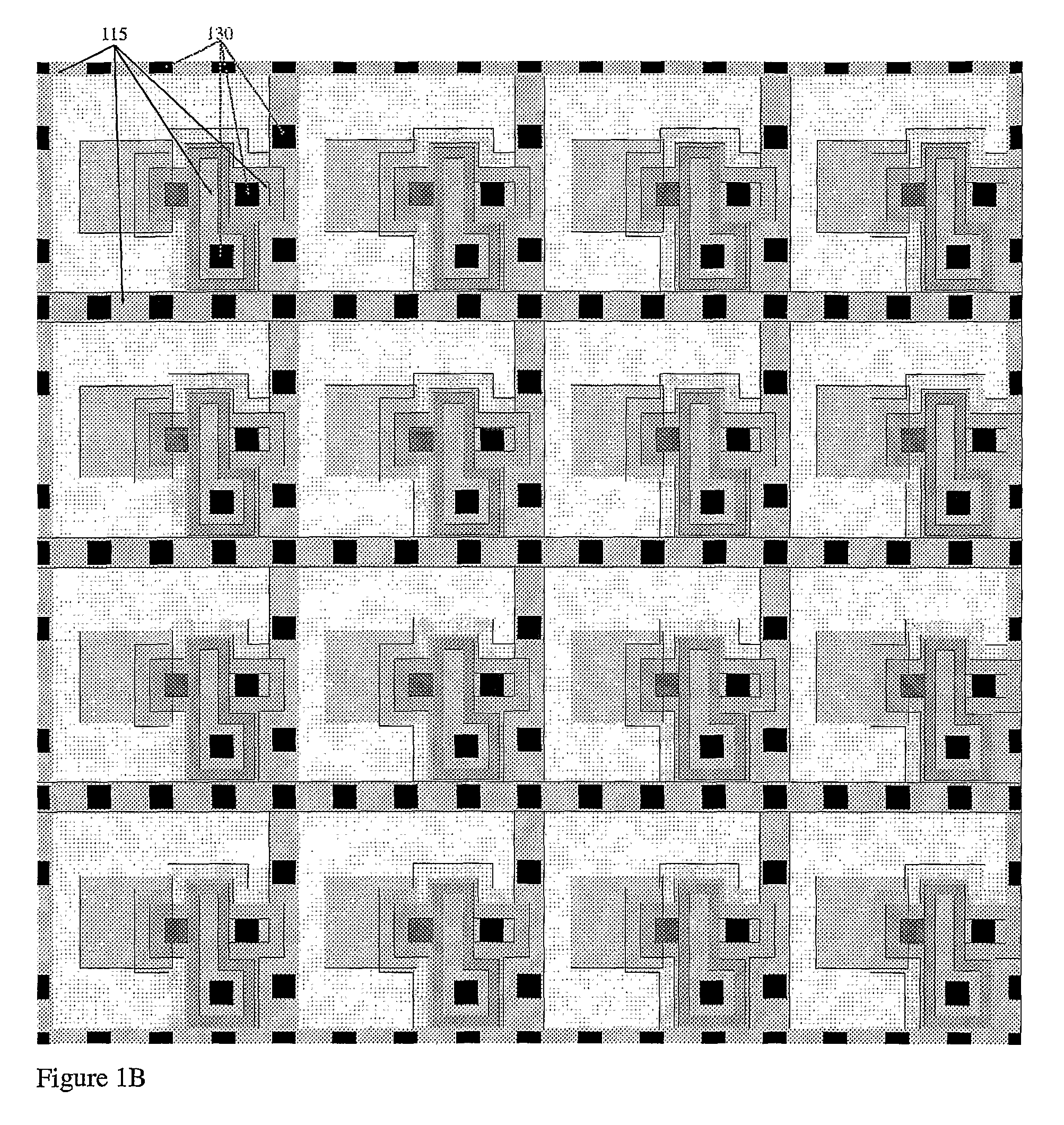
[0031]The present invention is based by the invention of WO 02 / 33755, which discloses a device and process architectures suitable for the monolithic integration of deep sub-micron CMOS technology, including sub-100 nm CMOS technology, with optoelectronic devices having active layers deposited on CMOS active areas. One example of such devices is an Avalanche Photo-Diode (APD) incorporating epitaxial SiGeC layers.
[0032]The device and process architectures disclosed in WO 02 / 33755 show how single-crystal p-type SiGe and / or SiGeC epitaxial films can be epitaxially deposited on n-type CMOS active areas, forming a pn-heterojunction that is separated, by shallow trench isolation (STI), from the neighboring CMOS devices. For this reason it can be run in the avalanche mode, unlike conventional CMOS junctions, thus unlike conventional CMOS photo-diodes. The p-type SiGe and / or SiGeC is the top electrode of the APD and the n-type CMOS active area is the bottom electrode of the APD. The top elec...
PUM
 Abstract
Description
Claims
Application Information