Check patentability & draft patents in minutes with Patsnap Eureka AI!

Multilayer printed circuit board having electromagnetic wave reduction member

a printed circuit board and electromagnetic wave technology, applied in the direction of cross-talk/noise/interference reduction, printed resistor incorporation, electrical apparatus construction details, etc., can solve the problems of reducing the signal-to-noise ratio reducing the reception sensitivity of the broadcasting receive antenna, etc., to reduce the radiation of electromagnetic waves

Active Publication Date: 2012-06-05
SAMSUNG ELECTRONICS CO LTD
View PDF14 Cites 2 Cited by
  • Summary
  • Abstract
  • Description
  • Claims
  • Application Information

AI Technical Summary

Benefits of technology

[0009]The present general inventive concept provides a multilayer printed circuit board capable of reducing an electromagnetic wave radiated around a sectional region of the multilayer printed circuit board.
[0011]The foregoing and / or other aspects and utilities of the present general inventive concept may be achieved by providing a multilayer printed circuit board including a power source surface to provide power to a plurality of electrical components, a ground surface having a reference voltage, a strip line formed to pass through the power source surface and / or the ground surface to transmit signals between at least two of the plurality of electrical components, an antenna disposed in proximity to a sectional region of the power source surface and the ground surface, and an electromagnetic wave reduction member which is provided between the power source surface and the ground surface in proximity to the antenna to reduce the electromagnetic wave generated from the strip line.
[0017]The foregoing and / or other aspects and utilities of the present general inventive concept may also be achieved by providing a multilayer printed circuit board including a power source surface to provide power to a plurality of components, a ground surface having a reference voltage, a strip line formed to pass through the power source surface and / or the ground surface to transmit signals between at least two of the plurality of components, and a capacitor and a resistor formed between the power source surface and the ground surface to reduce the scatter parameter of an electromagnetic wave generated from the strip line.
[0022]An interference effect on the antenna caused by an electromagnetic wave generated around the strip line may be effectively reduced.

Problems solved by technology

In this case, a receive sensitivity of the broadcasting receive antenna is degraded due to interference from the electromagnetic wave that radiates around the sectional region of the multilayer printed circuit board.
That is, in the broadcasting receiver, the broadcasting receive antenna is generally placed around the sectional region of the multilayer printed circuit board due to the structure of the product, and in this case, the electromagnetic wave radiated around the sectional region of the multilayer printed circuit board causes interference, thereby lowering a signal-to-noise ratio of the broadcasting receive antenna.

Method used


Image

  • Multilayer printed circuit board having electromagnetic wave reduction member
  • Multilayer printed circuit board having electromagnetic wave reduction member
  • Multilayer printed circuit board having electromagnetic wave reduction member

Examples


Embodiment Construction

[0031]Reference will now be made in detail to the embodiments of the present general inventive concept, examples of which are illustrated in the accompanying drawings, wherein like reference numerals refer to the like elements throughout. The embodiments are described below in order to explain the present general inventive concept by referring to the figures.

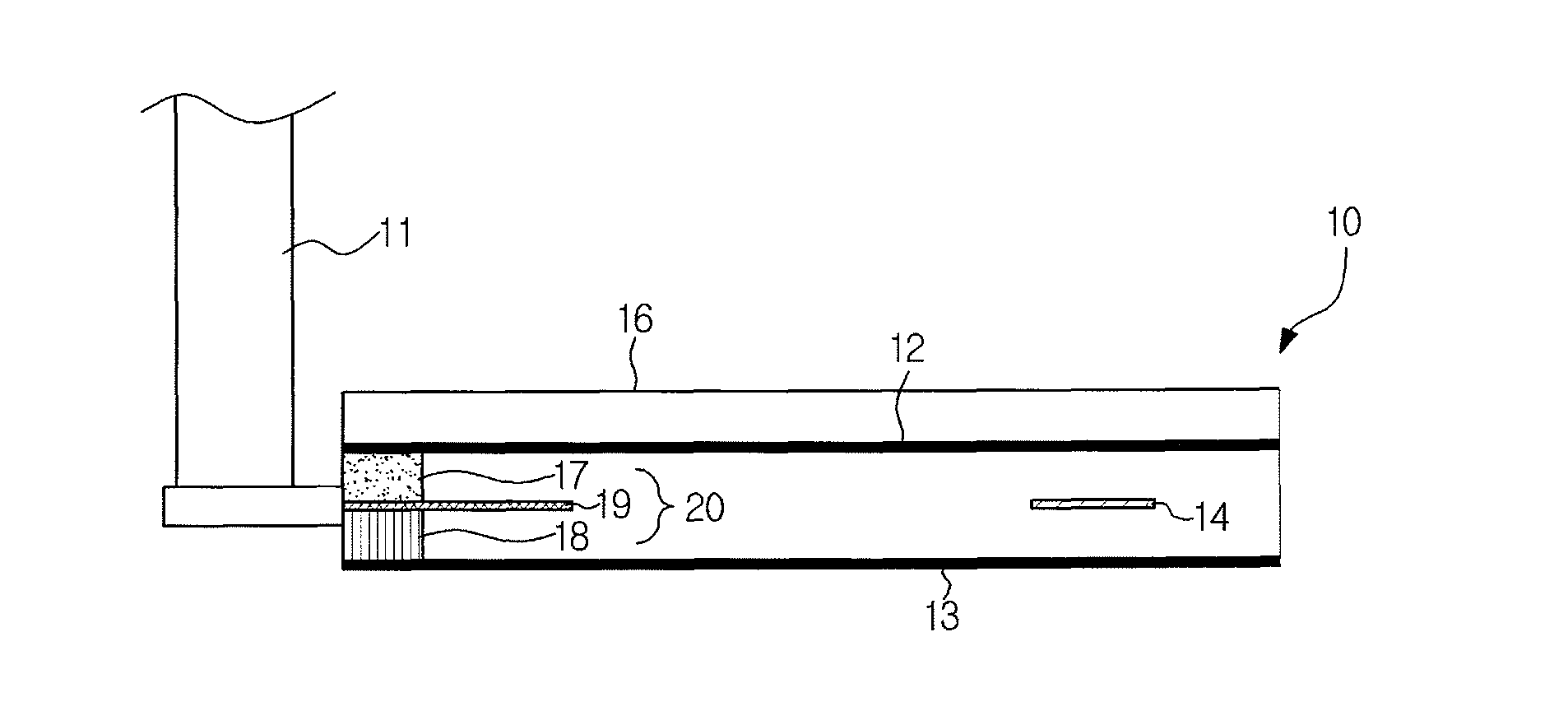
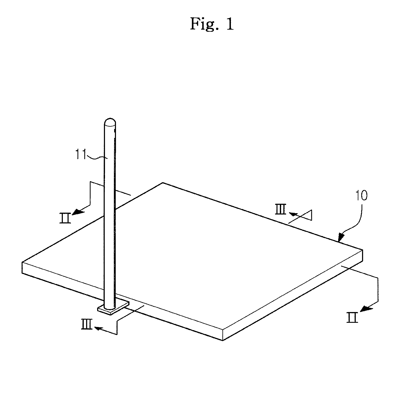
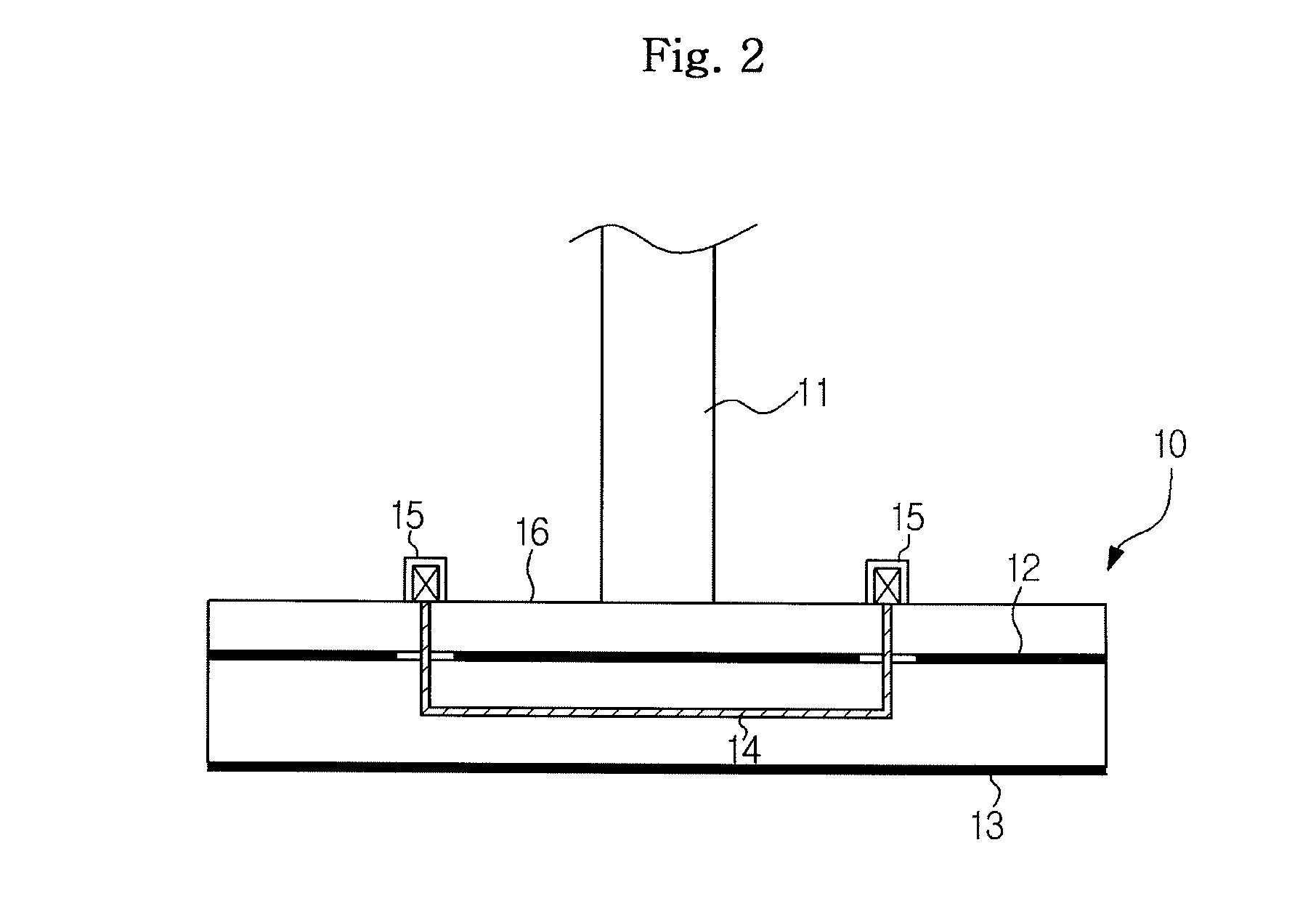
[0032]As illustrated in FIGS. 1 to 3, a multilayer printed circuit board 10 according to an embodiment of the present general inventive concept includes a mounting surface 16 on which various components 15 are mounted, a power source surface 12 to provide power to the components 15, and a ground surface 13 having a reference voltage.

[0033]In addition, the multilayer printed circuit board 10 according to the present general inventive concept further includes a broadcasting receive antenna 11 which is installed adjacent to the sectional region of the multilayer printed circuit board 10 so as to receive broadcasting signals, and a ...


PUM


Abstract

Disclosed is a multilayer printed circuit board. The multilayer printed circuit board includes a power source surface to provide power to each component disposed on the power source surface, a ground surface having a reference voltage, a strip line which passes through the power source surface and / or the ground surface so as to transmit signals between components, an antenna installed in proximity to a sectional region of the power source surface and the ground surface, and an electromagnetic wave reduction member which is provided between the power source surface and the ground surface to effectively reduce an electromagnetic wave generated from the strip line.

Description

CROSS-REFERENCE TO RELATED APPLICATIONS[0001]This application claims the benefit of Korean Patent Application No. 2007-16854 filed on Feb. 16, 2007, in the Korean Intellectual Property Office, the disclosure of which is incorporated herein by reference in its entirety.BACKGROUND OF THE INVENTION[0002]1. Field of the Invention[0003]The present general inventive concept relates to a multilayer printed circuit board, and more particularly to a multilayer printed circuit board capable of reducing an electromagnetic wave radiated within a sectional region of the multilayer printed circuit board.[0004]2. Description of the Related Art[0005]In general, a multilayer printed circuit board refers to a printed circuit board including a plurality of layers. As disclosed in Korean Unexamined Patent Publication No. 2006-93519 (electromagnetic wave shielding structure in multilayer printed circuit board), a conventional multilayer printed circuit board includes a top surface of a first layer and a...

Claims


Application Information

Patent Timeline
Patent Type & Authority Patents(United States)
IPC IPC(8): H05K9/00
CPCH05K1/0234H05K1/162H05K1/167H05K2201/09309H05K2201/09336H05K3/46
Inventor PARK, HARK BYEONGSEOL, BYONG SUKIM, HYUNG GEUNPARK, HYUN HOLEE, JONG SUNGLEE, HYUNG SEOKMOON, YOUNG JUN
Owner SAMSUNG ELECTRONICS CO LTD
Features
  • R&D
  • Intellectual Property
  • Life Sciences
  • Materials
  • Tech Scout
  • Unparalleled Data Quality
  • Higher Quality Content
  • 60% Fewer Hallucinations
Learn More