
OLED with high efficiency blue light-emitting layer

a blue light-emitting layer, high-efficiency technology, applied in the direction of thermoelectric devices, discharge tube luminescnet screens, natural mineral layered products, etc., can solve the problems of reducing the efficiency of the color-complementary layer(s) in the white oled, reducing the efficiency of the color-complementary layer(s) and the blue lifetime, and reducing the efficiency of the blue lifetime. , to achieve the effect of reducing the cost of production,

Active Publication Date: 2012-08-14
GLOBAL OLED TECH
View PDF41 Cites 3 Cited by
  • Summary
  • Abstract
  • Description
  • Claims
  • Application Information

AI Technical Summary

Benefits of technology

[0011]Devices of the invention provide improved features such as increased efficiency while maintaining sufficient operational stability and excellent color characteristics.

Problems solved by technology

While organic electroluminescent (EL) devices have been known for over two decades, their performance limitations have represented a barrier to many desirable applications.
Such improvements in blue light emitting layers are particularly beneficial for white-light-producing OLEDs since blue light emitters tend to have lower efficiencies than emitters of other colors, so that in order to produce balanced whites, the blue pixel (in a RGB OLED device) may need to be driven at higher current densities, resulting in increased power consumption as well as shortened blue lifetimes, and the color-complementary layer(s) (in a white OLED) may need to operate at less than their maximum potential efficiency.
However, these devices do not necessarily have all desired EL characteristics in terms of high luminance, low drive voltage, and sufficient operational stability.

Method used


Image

  • OLED with high efficiency blue light-emitting layer
  • OLED with high efficiency blue light-emitting layer
  • OLED with high efficiency blue light-emitting layer

Examples


experimental examples

[0089]The following table lists LUMO values for selected materials used in the following experiments. TPBI is 2,2′,2″-(1,3,5-benzenetriyl)tris[1-phenyl-1H-benzimidazole]. Alq is tris(quinolin-8-olato)aluminum(III). BAlq′ is bis(2-methylquinolin-8-olato)(2,6-diphenyl-phenolato)aluminum(III). CH-1 is bis(9,9′-spirobifluorene-2-yl) ketone.

[0090]

TABLE AExperimentally-determined (column 2) and calculated(column 3) LUMO energies for selected materials.MaterialLUMO expLUMO calcA-1−2.52−2.53A-2−2.44−2.46A-3−2.45−2.45A-4−2.45−2.46A-5−2.40−2.40CBP−1.96−2.13CH-1−2.42−2.50Alq−2.50−2.51N-1−1.95−2.03B-1−1.60B-2 (mCP)−1.78−1.75NPB−1.93−2.06B-3−2.21B-4−2.13−2.13Ir(ppy)3−2.04−2.10Bphen−2.40−2.29TPBI−2.27−2.09BAlq′−2.42−2.50F-1−2.57−2.61

example series 1

[0091]EL devices 1-1 to 1-36 were constructed in the following manner:[0092]1. A glass substrate, coated with an approximately 25 nm layer of indium-tin oxide (ITO) as the anode, was sequentially ultrasonicated in a commercial detergent, rinsed in deionized water, dried and exposed to oxygen plasma for about 1 minute.[0093]2. Over the ITO a 1 nm fluorocarbon (CFx) hole injecting layer (HIL1) was deposited by plasma-assisted deposition of CHF3 as described in U.S. Pat. No. 6,208,075.[0094]3. A 10 nm layer of dipyrazino[2,3-f:2′,3′-h]quinoxaline-2,3,6,7,10,11-hexacarbonitrile (HAT-CN) was then vacuum-deposited as a second hole-injection layer (HIL2).[0095]4. Next, a hole transporting layer (HTL) of N,N′-di-1-naphthyl-N,N′-diphenyl-4,4′-diaminobiphenyl (NPB) was vacuum-deposited to a thickness of 75 nm.[0096]5. A 25 nm light emitting layer including A-4 and 7% S-2 was then vacuum-deposited onto the HTL.[0097]6. A thin first ETL (ETL1) was vacuum-deposited over the LEL with thickness an...

example series 2

[0105]EL devices 2-1 to 2-9 were constructed in the same manner as Example Series 1 except that the material in the LEL was varied according to Table 2. CBP is 4,4′-bis(N-carbazolyl)-1,1′-biphenyl. Devices were aged electrically at room temperature at a constant current density of 80 mA / cm2 (DC mode). The lifetime (T50), or operational stability, of an OLED device is defined as the number of hours required for the luminance at 80 mA / cm2 to drop to half the luminance of the fresh device.

[0106]

TABLE 2ETL1 Variations with Anthracene and Non-AnthraceneLEL Host and Anthracene A-1 in ETL2ETL1LELThicknessT50 at 80ExamplehostETL1(nm)Vcd / AEQEmA / cm21-1A-1NoneNone3.28.36.5165(Comp)1-2A-1N-10.53.18.206.4175(Comp)1-3A-1N-11.53.310.38.0147(Inv)1-4A-1N-12.53.512.29.4111(Inv)1-5A-1N-13.53.710.48.174(Inv)1-6A-1N-15.04.57.76.0102(Comp)1-10A-1mCp1.53.311.98.6162(Inv)1-11A-1mCp2.53.412.49.1168(Inv)1-12A-1mCp3.53.412.69.2125(Inv)2-1CBPNoneNone5.03.52.727(Comp)2-2CBPN-11.54.94.73.424(Comp)2-3CBPN-12.55.2...


PUM

PropertyMeasurementUnit
thickaaaaaaaaaa
thickaaaaaaaaaa
LUMOaaaaaaaaaa

Abstract

The invention provides an OLED device comprising an anode, a cathode and a light-emitting layer located therebetween, said light-emitting layer comprising an anthracene host and a styrylamine blue light-emitting compound; and, located between the said light-emitting layer and the cathode, a first electron-transporting layer that is greater than 0.5 nm and less than 5 nm thick; and a second electron-transporting layer consisting essentially of an anthracene located between the first electron-transporting layer and the cathode. The first electron-transporting layer includes a compound with a less negative LUMO level than the anthracene in the second electron-transporting layer. Devices of the invention provide improvement in features such as efficiency.

Description

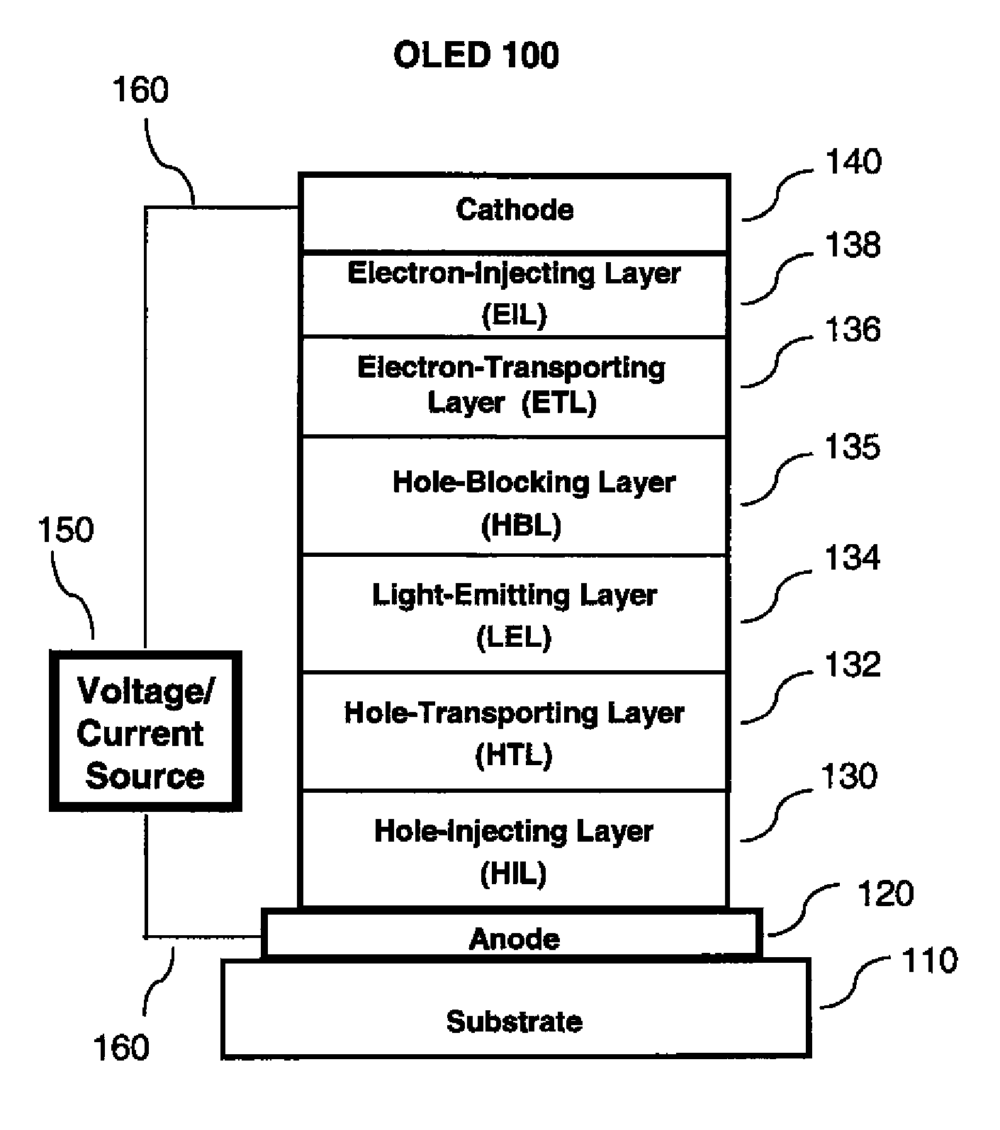
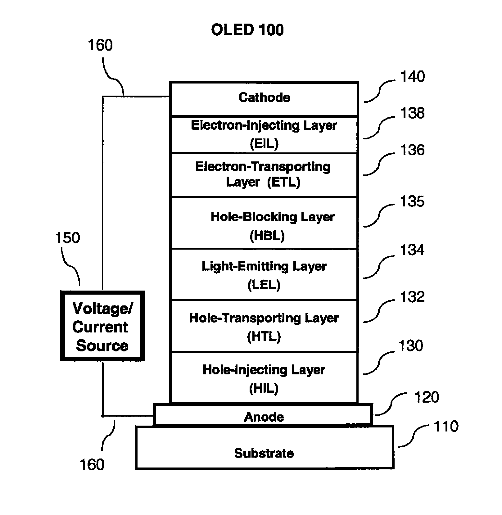
FIELD OF THE INVENTION[0001]This invention relates to an electroluminescent device, more specifically, an organic light-emitting diode (OLED) device having a light-emitting layer containing a blue light-emitting styrylamine compound and an anthracene host; a thin first electron-transporting layer; and a second electron-transporting layer consisting essentially of an anthracene. The first electron-transporting layer contains a compound with a LUMO level less negative than the LUMO level of the anthracene of the second electron-transporting layer.BACKGROUND OF THE INVENTION[0002]While organic electroluminescent (EL) devices have been known for over two decades, their performance limitations have represented a barrier to many desirable applications. In their simplest forms, organic light-emitting diodes (OLEDs), also referred to as organic electroluminescent devices, contain spaced electrodes separated by an organic light-emitting structure which emits light in response to the applicat...

Claims


Application Information

Patent Timeline
Patent Type & Authority Patents(United States)
IPC IPC(8): H01L29/08
CPCH01L51/5004H01L51/5012H01L2251/552H10K85/615H10K85/631H10K85/342H10K50/11H10K2101/40H10K50/166H10K2101/30H10K50/16
Inventor KONDAKOVA, MARINA E.YOUNG, RALPH H.
Owner GLOBAL OLED TECH
Learn More